
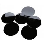
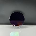
3 Inch InP Crystal Dummy Prime Semiconductor Substrate

Products Detailed
3 Inch InP Crystal Dummy Prime Semiconductor Substrate2inch InP wafers 3inch 4inch N/P TYPE InP Semiconductor Substrate Wafers Doped S+/ Zn+ /Fe + growth (modified VFG method) is used to pull a single ... |
| [View Products Detailed] |
| Product Tags: Dummy Prime Semiconductor Substrate InP Crystal Semiconductor Substrate SSP Semiconductor Substrate |
Related Products
|
Semi Insulating GaN-On-Silicon Wafer Free Standing Gallium Nitride Substrates |
|
1inch 2inch Beta Coefficient Ga2O3 Gallium Oxide Wafer Substrate Dsp Ssp |
|
Beta Coefficient-Ga2O3 Gallium Oxide Wafer Doped Mg Fe3+ Square Substrate Dsp Ssp |

|
Large Thickness SiO2 Thermal Oxide On Silicon Wafers For Optical Communication System |
|
Y-42 Degree 4inch Lithium Tantalate LiTaO3 LiNbO3 Lithium Niobate Crystal Raw Unprocessed Ingots |

|
Single Crystal InP Indium Phosphide Wafers 350 - 650um Thickness |
Email to this supplier