
1 - 10 of 189
dummy prime semiconductor substrate
Selling leads
|
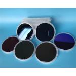
2inch InP wafers 3inch 4inch N/P TYPE InP Semiconductor Substrate Wafers Doped S+/ Zn+ /Fe + growth (modified VFG method) is used to pull a single ...
2025-05-06 20:44:37
|
|
...substrates wafers/4 inch 4h-N type SIC Substrates 0.35 mm DSP Prime Zero Grade Silicon Carbide Wafer About Silicon Carbide (SiC)Crystal Silicon ...
2025-07-30 00:08:00
|
|
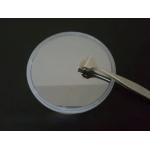
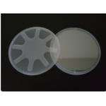
...Semiconductor Substrate For Epitaxial Growth VGF 2inch 4inch 6inch n-type prime grade GaAs wafer for epitaxial growth Gallium arsenide can be made ...
2025-05-06 20:45:00
|
|
...thickness 500±25um n doped dummy prime research grade 8inch 12inch 4H-N type SiC Wafer's abstract This study presents the characterization of an 8...
2025-05-06 20:41:22
|
|
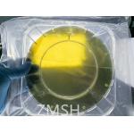
...prime grade GaAs wafer for epitaxial growth GaAs wafer (Gallium Arsenide) is an advantageous alternative to silicon that has been evolving in the ...
2025-05-06 20:44:45
|
|
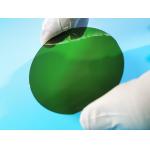
... Substrate Indium Arsenide InAs wafer Application Indium Arsenide (InAs) single crystal semiconductor substrates are materials with unique ...
2025-07-30 00:08:00
|
|
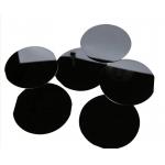
... Grade About Silicon Carbide (SiC)Crystal Silicon carbide (SiC), also known as carborundum, is a semiconductor containing silicon and carbon with ...
2025-05-06 20:40:56
|
|
... GaAs Wafer Product Description (GaAs) Gallium Arsenide Wafers PWAM Develops and manufactures compound semiconductor substrates-gallium arsenide ...
2025-05-06 20:44:31
|
|
2inch InP wafers 3inch 4inch N/P TYPE InP Semiconductor Substrate Wafers Doped S+/ Zn+ /Fe + growth (modified VFG method) is used to pull a single ...
2025-05-06 20:44:36
|
|
...substrate, and an infrared light-emitting device with a wavelength of 2 to 14 μm can be fabricated. The AlGaSb superlattice structure material can ...
2025-05-06 20:44:36
|