
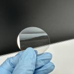
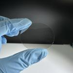
6N Purity DSP Surface Undoped HPSI Dummy Prime Grade SIC Wafer
|
|
Customzied size/2inch/3inch/4inch/6inch 6H-N/4H-SEMI/ 4H-N SIC ingots/High purity 4H-N 4inch 6inch dia 150mm silicon carbide single un-doped 4" 6" 6inch 4h-semi sic wafer 4Inch production dummy Grade
About Silicon Carbide (SiC)Crystal Silicon carbide (SiC), also known as carborundum, is a semiconductor containing silicon and carbon with chemical formula SiC. SiC is used in semiconductor electronics devices that operate at high temperatures or high voltages, or both.SiC is also one of the important LED components, it is a popular substrate for growing GaN devices, and it also serves as a heat spreader in high-power LEDs.
1. Description
4H-N 4inch diameter Silicon Carbide (SiC) Substrate Specification
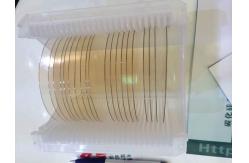
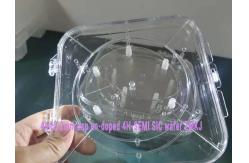
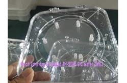
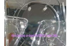
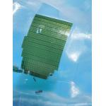
Production display show
CATALOGUE COMMON SIZE In OUR INVENTORY LIST
SiC Applications Application areas
1. High-Power Electronic Devices Due to its superior thermal conductivity, high breakdown voltage, and wide bandgap, 6N purity undoped HPSI SiC wafers are ideal for high-power electronic devices. These wafers can be used in power electronics such as diodes, MOSFETs, and IGBTs for applications like electric vehicles, renewable energy systems, and power grid management, enabling efficient power conversion and reducing energy losses. 2. Radio Frequency (RF) and Microwave DevicesHPSI SiC wafers are essential for RF and microwave devices, particularly for use in telecommunications, radar, and satellite communication systems. Their semi-insulating nature helps in reducing parasitic capacitances and improving high-frequency performance, making them suitable for RF amplifiers, switches, and oscillators in wireless communication and defense technologies. 3. Optoelectronic DevicesSiC wafers are increasingly used in optoelectronic applications, including UV detectors, LEDs, and lasers. The 6N purity undoped wafers provide superior material characteristics that enhance the performance of these devices, particularly in harsh environments where conventional silicon-based devices would fail. Applications include medical diagnostics, military equipment, and industrial sensing. 4. Wide Bandgap Semiconductors for Harsh EnvironmentsSiC wafers are known for their ability to function in extreme temperatures and high-radiation environments. These characteristics make 6N purity SiC wafers perfect for aerospace, automotive, and defense industries, where devices need to operate under harsh conditions, such as in spacecraft, high-temperature engines, or nuclear reactors. 5. Research and DevelopmentAs a dummy prime-grade wafer, this type of SiC wafer is used in R&D environments for testing and calibration purposes. Its high purity and polished surface make it ideal for validating processes in semiconductor fabrication, testing new materials, and developing new semiconductor devices without the need for active doping. It's frequently used in academic and industrial research labs for studies in materials science, device physics, and semiconductor engineering. 6. High-Frequency Switching DevicesSiC wafers are commonly utilized in high-frequency switching devices for applications in power management systems. Their wide bandgap and semi-insulating properties make them highly efficient for handling fast switching speeds with reduced power losses, which are critical in systems like inverters, converters, and uninterruptible power supplies (UPS). 7. Wafer-Level Packaging and MEMSThe DSP surface of the SiC wafer allows for precise integration into wafer-level packaging and micro-electromechanical systems (MEMS). These applications require extremely smooth surfaces for high-resolution patterning and etching, making the polished surface of the 6N purity wafer a crucial feature. MEMS devices are commonly used in sensors, actuators, and other miniaturized systems for automotive, medical, and consumer electronics applications. 8. Quantum Computing and Advanced ElectronicsIn cutting-edge applications like quantum computing and next-generation semiconductor devices, the undoped HPSI SiC wafer serves as a stable and highly pure platform for building quantum devices. The high purity and semi-insulating properties make it an ideal material for hosting qubits and other quantum components. In conclusion, the 6N purity DSP surface, undoped HPSI Dummy Prime Grade SiC wafer is an essential material for a wide range of applications, including high-power electronics, RF devices, optoelectronics, quantum computing, and advanced research. Its high purity, semi-insulating properties, and polished surface enable superior performance in challenging environments and contribute to advancements in both industrial and academic research. >Packaging – Logistcs
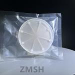
According to the quantity and shape of the product , we will take a different packaging process! Almost by single wafer cassettes or 25pcs cassette in 100 grade cleaning room. FAQ Q1. Are you a factory? A1. Yes, we are a professional manufacturer of optical components,
we have more than 8years experience in wafers and optical lens
process. Q2. What is the MOQ of your products? A2. No MOQ for customer if our product is in stock, or 1-10pcs. Q3:Can I custom the products based on my requirement? A3.Yes, we can custom the material, specifications and optical
coating for youroptical components as your requirement. Q4. How can I get sample from you? A4. Just send us your requirements, then we will sendsamples
accordingly. Q5. How many days will samples be finished? How about mass
products? A5. Generally, we need 1~2weeks to finish the sample production. As
for the mass products, it depends on your order quantity. Q6. What's the delivery time? A6. (1)For inventory: the delivery time is 1-3 working days. (2)
For customized products: the delivery time is 7 to 25 working days. According to the quantity. Q7. How do you control the quality? A7. More than four times quality inspect during production
process,we can provide the Quality test report. Q8. How about your optical lens production ability per Month? A8. About 1,000pcs/Month.According to the detail requirement.
|
||||||||||||||||||||||||||||||||||||||||||||||||||||||||||||||||||||||||||||||||||||||||||||||||||||||||||||||||||||||||||||||||||||||||||||||||||||||||||||||||||||||||||||||||||||||||||||||||||||||||||||||||||||||||||||||||||||||||||||||||||||||||||||||||||||||||||||||||||||||||||||||||||||||||||||||||
| Product Tags: carborundum Silicon wafer dummy grade Silicon wafer DSP monocrystalline silicon wafer | ||||||||||||||||||||||||||||||||||||||||||||||||||||||||||||||||||||||||||||||||||||||||||||||||||||||||||||||||||||||||||||||||||||||||||||||||||||||||||||||||||||||||||||||||||||||||||||||||||||||||||||||||||||||||||||||||||||||||||||||||||||||||||||||||||||||||||||||||||||||||||||||||||||||||||||||||
|
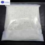
High Purity Semi-Insulating HPSI SiC Powder/99.9999% Purity Crystal Growth |
|
Semi-Insulating SiC Wafers 3inch 76.2mm 4H Type SiC For Semiconductors |
|
High Resistivity 8inch 200mm Silicon Carbide Wafer Production Grade 4H-N |
|
4H/6H Semi-Insulating Silicon Carbide Wafer For Production/Research/Dummy Grade |
|
Square SiC Windows Silicon Carbide Substrate 1x1x0.5mmt SiC Lens |
|
Semi Insulating Silicon Carbide Wafer SiC Substrate Orientation 0001 Bow/Warp ≤50um |