
1 - 10 of 215
ssp semiconductor substrate
Selling leads
|
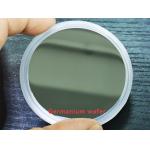
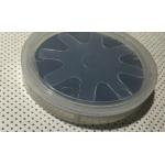
2inch N-type single side polished Ge wafers Germanium substrate Ge window for infrared Co2 lasers Diameter:25.4mm Thickness:0.325mm Shanghai Famous ...
2025-05-06 20:44:50
|
|
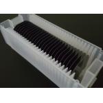
VFG metod N-type 2inch/3inch,4inch ,6inch dia150mm GaAs Gallium Arsenide Wafers N-type Semi-insulating type for Microelectronics, --------------------...
2025-05-06 20:44:31
|
|
VFG metod N-type 2inch/3inch,4inch ,6inch dia150mm GaAs Gallium Arsenide Wafers N-type Semi-insulating type for Microelectronics, --------------------...
2025-05-06 20:44:43
|
|
... to a silicon carbide (SiC) wafer with a 12-inch diameter (approximately 300mm), a size standard used in the semiconductor industry for the mass ...
2025-05-06 20:41:54
|
|
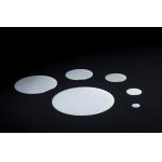
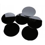
4inch 6inch 8inch 12inch sapphire Wafers epi-ready Prime grade DSP SSP sapphire substrates 8inch 200mm Ultra Thin sapphire wafers 0.1mm-50mm Thickness ...
2025-05-06 20:39:16
|
|
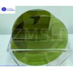
... Substrate Indium Arsenide InAs wafer Application Indium Arsenide (InAs) single crystal semiconductor substrates are materials with unique ...
2025-07-22 00:12:04
|
|
...Semiconductor Substrate For Epitaxial Growth VGF 2inch 4inch 6inch n-type prime grade GaAs wafer for epitaxial growth Gallium arsenide can be made ...
2025-05-06 20:45:00
|
|
... GaAs Wafer Product Description (GaAs) Gallium Arsenide Wafers PWAM Develops and manufactures compound semiconductor substrates-gallium arsenide ...
2025-05-06 20:44:31
|
|
2inch InP wafers 3inch 4inch N/P TYPE InP Semiconductor Substrate Wafers Doped S+/ Zn+ /Fe + growth (modified VFG method) is used to pull a single ...
2025-05-06 20:44:36
|
|
2inch InP wafers 3inch 4inch N/P TYPE InP Semiconductor Substrate Wafers Doped S+/ Zn+ /Fe + growth (modified VFG method) is used to pull a single ...
2025-05-06 20:44:37
|