
31 - 40 of 61
optoelectronics gallium nitride wafer
Selling leads
|
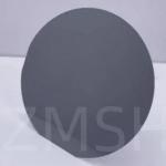
...wafer 2inch with OF Location/Length EJ 0-1-1 / 16±1mm LED LD Mobility Min 100 Product Description: A GaP wafer is a semiconductor substrate ...
2025-05-06 20:45:06
|
|
... (GaAs) Gallium Arsenide Wafers Gallium arsenide (GaAs) is a compound of the elements gallium and arsenic. It is a III-V direct bandgap semiconduct...
2025-05-06 20:44:43
|
|
...Gallium phosphide (GaP) crystals crystal substrate,GaP wafer ZMKJ can provides 2inch GaP wafer – gallium Phosphide which are grown by LEC(Liquid ...
2025-05-06 20:44:33
|
|
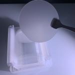
...Wafer SSP DSP Product Description: Sapphire bonding sheet is used for thinning and polishing of gallium arsenide wafers Due to the weight and ...
2025-07-26 00:07:38
|
|
2inch 4inch 6inch 8inch 3C-N SiC Wafer Silicon Carbide Optoelectronic High-Power RF LEDS Description of 3C-N SiC Wafer: Compared to 4H-Sic, although ...
2025-05-06 20:41:48
|
|
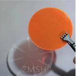
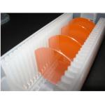
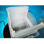
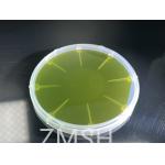
...-yellow semitransparent crystal material with an indirect band gap of 2.26 eV (300K), which is synthesized from 6N 7N high purity gallium and ...
2025-05-06 20:45:06
|
|
..., optoelectronic devices, semiconductor devices, and other fields. The high light transmittance and high hardness of sapphire wafers make them ...
2025-07-26 00:07:39
|
|
...Wafers 3C-N type 5*5 & 10*10mm inch diameter thickness 350 μm±25 μm Silicon Carbide Wafers 3C-N type's abstract This abstract introduces Silicon ...
2025-05-06 20:41:44
|
|
...wafer 4H N-Type CVD Orientation : 4.0°±0.5° Semi-Insulating 3-Inch Silicon Carbide wafer's Abstract The unique electronic and thermal properties of ...
2025-05-06 20:41:19
|
|
Semi-Insulating SiC Composite Substrates Epi ready 6inch 150mm for optoelectronic devices Summary for Semi-Insulating SiC Composite Substrates The ...
2025-05-06 20:41:34
|