
41 - 50 of 61
optoelectronics gallium nitride wafer
Selling leads
|
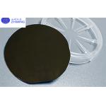
10x10mmt Terbium gallium garnet (TGG)crystals substrate wafer for laser device Product Type: Terbium gallium garnet (TGG) crystal substrateProduct ...
2025-05-06 20:40:28
|
|
VGF 2 Inch 4Inch N Type P Type GaAs Wafer Semiconductor Substrate For Epitaxial Growth VGF 2inch 4inch 6inch n-type prime grade GaAs wafer for ...
2025-05-06 20:45:00
|
|
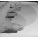
...Silicon Wafers Ultra-High Purity Optoelectronic-Grade Abstract The high-purity silicon wafer we offer undergoes precision machining and strict ...
2025-05-06 20:45:04
|
|
... innovation. Crafted from pristine indium phosphide, a binary semiconductor renowned for its superior electron velocity, our wafer offers ...
2025-05-06 20:45:10
|
|
...wafer for FP laser diode N-InP substrate FP Epiwafer's Overview Our N-InP Substrate FP Epiwafer is a high-performance epitaxial wafer designed for ...
2025-05-06 20:45:35
|
|
10x10mmt Terbium gallium garnet (TGG)crystals substrate wafer for laser device Product Type: Yttrium aluminum garnet (YAG) is an isotropic crystal ...
2025-07-23 00:09:03
|
|
... growth 430um SSP DSP About synthetic sapphire crystal Due to the less mismatched lattice and stable chemical and physical properties, sapphire...
2025-07-23 00:09:03
|
|
... wafer Applications of AlN template Silicon-based semiconductor technology has reached its limits and could not satisfy the requirements of future ...
2025-05-06 20:44:39
|
|
...Silicon LiNbO3 Lithium Niobate Wafer Thin Films Layer On Silicon Substrate Lithium niobate (LiNbO3) crystal is an important photoelectric material, ...
2025-05-06 20:44:57
|
|
ZnTe: ZnTe wafer, ZnTe crystal Type N, Type P, Custom Sizes and Specifications Available Abstract of ZnTe Zinc telluride (ZnTe) is a direct bandgap ...
2025-05-06 20:45:56
|