
51 - 60 of 61
optoelectronics gallium nitride wafer
Selling leads
|
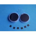
2-4inch Gallium antimonide GaSb Substrate Single Crystal Monocrystal for Semiconductor InAsSb/In-AsPSb, InNAsSb and other heterojunction materials can ...
2025-05-06 20:44:36
|
|
.../Green LED Wafer Flat or PPS Sapphire MOCVD DSP SSP Description of GaN-on-Sapphire Blue/Green LED Wafer: GaN on Sapphire (GaN/Sapphire) wafers ...
2025-05-06 20:44:26
|
|
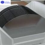
2inch 4inch 4" 2'' Sapphire based GaN templates GaN film on the sapphire substrate GaN-On-Sapphire GaN wafers GaN substrates GaN windows Properties of ...
2025-05-06 20:44:20
|
|
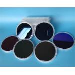
...Sapphire The growth of superconducting compounds / Gallium Nitride Infrared detectors Hybrid microelectronics Polishing carriers Hostile environmen...
2025-05-06 20:37:41
|

|
... application Application Sapphire wafer and substrate applications include: Microelectronic IC applications SOS Silicon-on-Sapphire The growth of ...
2025-05-06 20:37:41
|
|
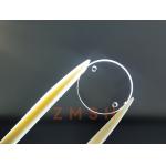
... Substrate Indium Arsenide InAs wafer Application Indium Arsenide (InAs) single crystal semiconductor substrates are materials with unique ...
2025-07-23 00:09:03
|
|
...wafer for epitaxial growth GaAs wafer (Gallium Arsenide) is an advantageous alternative to silicon that has been evolving in the semiconductor ...
2025-05-06 20:44:45
|
|
8inch GaN-on-Si Epitaxy si substrate(110 111 110)for MOCVD Reactors or RF energy application 8inch GaN-on-Si Epitaxy's abstract The 8-inch GaN-on-Si ...
2025-05-06 20:45:22
|
|
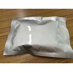
Product Introduction HPSI SiC powder (High Purity Semi-Insulating Silicon Carbide) is a high-performance material widely used in power electronics, ...
2025-07-23 00:09:03
|
|
... and optoelectronics due to their wide bandgap, high electron mobility, and thermal conductivity. These substrates leverage silicon's cost...
2025-05-06 20:45:21
|