
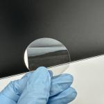
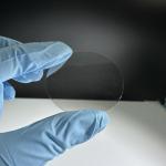
Semi-Insulating SiC Composite Substrates Epi Ready 6inch 150mm For Optoelectronic Devices
|
|
Semi-Insulating SiC Composite Substrates Epi ready 6inch 150mm for optoelectronic devices
Summary for Semi-Insulating SiC Composite SubstratesThe Semi-Insulating SiC Composite Substrates, designed for optoelectronic devices, offer superior performance with their exceptional properties. The polytype of these substrates is 4H, known for its excellent electronic and thermal properties. With a resistivity of ≥1E8 ohm·cm, these substrates ensure minimal leakage current and reduced electronic noise, crucial for high-precision applications.
A key feature is the transfer layer thickness, which is ≥0.4μm, providing a robust platform for epitaxial layer growth. The substrates exhibit a very low void density, with voids ≤5 per wafer for sizes between 0.5mm and 2mm in diameter. This low defect density ensures high reliability and performance consistency in device fabrication.
These substrates are particularly suitable for high-power and high-frequency optoelectronic devices due to their high breakdown voltage and superior thermal conductivity. The SiC material's high mechanical strength and chemical stability make it ideal for use in harsh environments, ensuring longevity and durability of the devices. Overall, these Semi-Insulating SiC Composite Substrates are engineered to meet the stringent demands of modern optoelectronic applications, providing a reliable foundation for the development of advanced electronic and photonic devices.
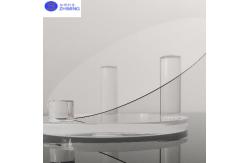
Specifications and Schematic Diagram for Semi-Insulating SiC Composite Substrates
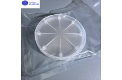
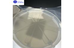
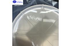
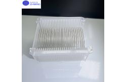
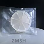
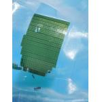
Semi-Insulating SiC Composite Substrates photo exhibition
Semi-Insulating SiC Composite Substrates application
Semi-insulating silicon carbide (SiC) composite substrates have numerous applications across various high-performance and advanced technology fields. Here are some key areas where they are particularly valuable:
By leveraging the unique properties of semi-insulating SiC, including its high thermal conductivity, wide bandgap, and chemical stability, engineers and researchers can develop devices that meet the demanding requirements of these advanced applications.
Q&A
Q:What is semi-insulating SiC?
A:Semi-insulating silicon carbide (SiC) is a type of silicon carbide material that has been engineered to have high electrical resistivity. This characteristic makes it an excellent substrate for the fabrication of high-frequency and high-power electronic devices, such as gallium nitride (GaN) transistors and diodes. Unlike conductive SiC, semi-insulating SiC minimizes parasitic conduction, reducing interference and improving device performance. This material achieves its semi-insulating properties through the introduction of specific dopants or defects that compensate for free charge carriers. Its thermal conductivity and mechanical strength also make it suitable for applications in harsh environments, such as power electronics and telecommunications. |
| Product Tags: 6inch SiC Composite Substrates Epi ready SiC Composite Substrates 150mm SiC Composite Substrates |
|
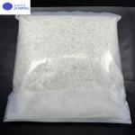
High Purity Semi-Insulating HPSI SiC Powder/99.9999% Purity Crystal Growth |
|
Semi-Insulating SiC Wafers 3inch 76.2mm 4H Type SiC For Semiconductors |
|
High Resistivity 8inch 200mm Silicon Carbide Wafer Production Grade 4H-N |
|
4H/6H Semi-Insulating Silicon Carbide Wafer For Production/Research/Dummy Grade |
|
Square SiC Windows Silicon Carbide Substrate 1x1x0.5mmt SiC Lens |
|
Semi Insulating Silicon Carbide Wafer SiC Substrate Orientation 0001 Bow/Warp ≤50um |