
171 - 180 of 303
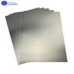
high purity silicon wafers
Selling leads
|
...Wafer Characteristic III-Nitride(GaN,AlN,InN) Gallium Nitride is one kind of wide-gap compound semiconductors. Gallium Nitride (GaN) substrate is a ...
2025-05-06 20:44:18
|
|
...Wafer Characteristic III-Nitride(GaN,AlN,InN) Gallium Nitride is one kind of wide-gap compound semiconductors. Gallium Nitride (GaN) substrate is a ...
2025-05-06 20:44:18
|
|
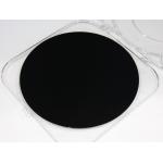
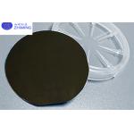
Abstract The 4-H Semi-Insulating SiC substrate is a high-performance semiconductor material with a wide range of applications. It derives its name ...
2025-05-06 20:41:16
|
|
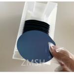
SiO2 wafer Thermal Oxide Laver Thickness 20um+5% MEMS Optical Communication System Product Description: The SIO2 silicon dioxide wafer serves as a ...
2025-05-06 20:45:05
|
|
Ni Substrate single crystal cubic structure a=3.25A purity 99.99% density 8.91 Ni Substrate's abstract Nickel (Ni) substrates, particularly in the ...
2025-05-06 20:45:48
|
|
..., optoelectronic devices, semiconductor devices, and other fields. The high light transmittance and high hardness of sapphire wafers make them ...
2025-07-24 00:12:37
|
|
... Thickness C-plane DSP Sapphire wafer 12inch sapphire wafers dia300mm DSP C-plane wafers BF33, Quartz wafers FEATURES OF SINGLE CRYSTAL SAPPHIRE 1. ...
2025-05-06 20:39:01
|
|
...InP substrate bandwidth 02:2.5G wavelength 1270nm epi wafer for FP laser diode N-InP substrate FP Epiwafer's Overview Our N-InP Substrate FP ...
2025-05-06 20:45:35
|
|
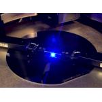
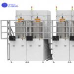
...6inch 8inch 12inch SiC wafers manufacture SiC single crystal growth furnace's abstract ZMSH is proud to offer the SiC single crystal growth furnace...
2025-05-06 20:43:51
|
|
...Wafer DSP Notch High Precision 8inch/6inch/5inch/ 2inch /3inch 4inch /5inch C-axis/ a-axis/ r-axis/ m-axis 6"/6inch dia150mm C-plane Sapphire SSP...
2025-05-06 20:39:17
|