
131 - 140 of 303
high purity silicon wafers
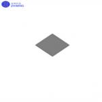
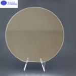
Selling leadsMg Substrate Magnesium Single Crystal Hexagonal 5x5x0.5/1mm 10x10x0.5/1mm20x20x0.5/1mm Purity 99.99%
|
... and hexagonal lattice structures are becoming increasingly important in material science, particularly for applications requiring lightweight yet ...
2025-05-06 20:45:47
|
|
... wafer is a specialized type of wafer that combines the properties of silicon carbide and silicon materials. The wafer consists of a layer of semi...
2025-05-06 20:45:23
|
|
...insulator made of silicon dioxide or glass (hence the name "silicon on insulation lining", often referred to as SOI for short). Transistors built ...
2025-05-06 20:45:41
|

|
... process (KY process) for sapphire crystal growth is currently used by many companies in China to produce sapphire for the electronics and optics ...
2025-05-06 20:39:27
|
|
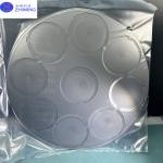
... for high-performance applications, particularly in the semiconductor industry. These trays play a critical role in the fabrication process of ...
2025-05-06 20:47:43
|
|
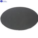
...Wafer 6inch 150mm SiC type 4H-N Si type N or P N-type SiC on Si Compound Wafer abstract N-type silicon carbide (SiC) on silicon (Si) compound ...
2025-05-06 20:45:18
|
|
...Wafer Carrier, Single Wafer Sample Box for Silicon, Sapphire, SiC Substrate Cleanroom Class 100 Grade 1 inch Style Single Wafer Carrier Shipper box ...
2025-05-06 20:47:34
|
|
...second-generation semiconductor materials represented by silicon (Si) and gallium arsenide (GaAs) has propelled the swift advancement of microelect...
2025-05-06 20:41:29
|
|
...Wafer with (111) Crystal Orientation – Introduction The 8-inch silicon wafer with (111) crystal orientation is a vital component in the semiconduct...
2025-05-06 20:45:52
|
|
...) are 3D integrated at the wafer scale. The two wafers are bonded face-to-face using a low-temperature oxide-oxide bonding technique. The Si ...
2025-05-06 20:44:26
|