
161 - 170 of 303
high purity silicon wafers
Selling leads
|
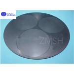
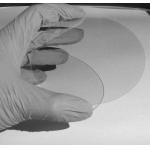
...Plate/Wafer Holder for ICP Etching Process Used in Epitaxial Growth Processing Abstract of SiC (Silicon Carbide) Ceramic Trays Silicon carbide (SiC...
2025-05-06 20:47:48
|
|
...Wafer (Lithium Niobate on Insulator)2/3/4/6/8 Inch Si/LN Substrate Introduction of LNOI Wafer LNOI (Lithium Niobate on Insulator) wafers are a ...
2025-06-30 20:10:46
|
|
... industries, owing to their unique material properties. With a wide bandgap, high electron mobility, and exceptional thermal stability, GaN wafers ...
2025-05-06 20:44:25
|
|
300-900nm LN-On-Silicon LiNbO3 Lithium Niobate Wafer Thin Films Layer On Silicon Substrate Lithium niobate (LiNbO3) crystal is an important photoelect...
2025-05-06 20:44:57
|
|
...wafer Applications of AlN template Silicon-based semiconductor technology has reached its limits and could not satisfy the requirements of future ...
2025-05-06 20:44:39
|
|
...WAFER WINDOW for OPTICAL LASER OPTICS APPLICATIONS High hardness Ir Optical Standard Window Multiple shapes sapphire window Optical Glass BK7...
2025-07-24 00:12:37
|
|
...Wafer Semiconductor Substrate For Epitaxial Growth VGF 2inch 4inch 6inch n-type prime grade GaAs wafer for epitaxial growth Gallium arsenide can be ...
2025-05-06 20:45:00
|
|
... technology, revolutionizing the landscape of advanced electronics. Comprising three distinct layers, this cutting-edge wafer embodies a trifecta ...
2025-05-06 20:45:07
|
|
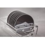
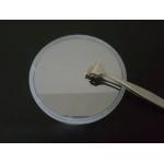
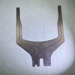
...wafers, optical component Abstract of SiC ceramic fork SiC Ceramic Fork Arm is a structural component made from advanced silicon carbide ceramic ...
2025-07-24 00:12:38
|
|
...wafer 1-5um AlN template 8inch 6inch AlGaN/GaN HEMT-on-HR Si Epiwafer GaN-on-Si Epiwafer for Micro-LED for RF application GaN Wafer Characteristic ...
2025-05-06 20:44:19
|