
GaN Gallium Nitride Wafer High Electron Mobility RF Devices Optoelectronics And LEDs
|
|
GaN Gallium Nitride Wafer High Electron Mobility RF Devices Optoelectronics and LEDs GaN Gallium Nitride Wafer's abstractGallium Nitride (GaN) wafers have emerged as a pivotal technology in various industries, owing to their unique material properties. With a wide bandgap, high electron mobility, and exceptional thermal stability, GaN wafers find applications in power electronics, RF devices, optoelectronics, and more. This abstract explores the versatile applications of GaN wafers, from powering 5G communications to illuminating LEDs and advancing solar energy systems. The high-performance characteristics of GaN make it a cornerstone in the development of compact and efficient electronic devices, influencing sectors such as automotive electronics, aerospace, and renewable energy. As a driving force in technological innovation, GaN wafers continue to redefine possibilities across diverse industries, shaping the landscape of modern electronics and communication systems. GaN Gallium Nitride Wafer's showcaseGaN Gallium Nitride Wafer's applicationGallium Nitride (GaN) wafers find a wide range of applications across multiple industries, leveraging their unique material properties for enhanced performance in electronic and optoelectronic devices. Here are some key applications of GaN wafers:
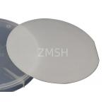
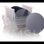
The diverse applications of GaN wafers underscore their significance in advancing technology across multiple sectors. The material's unique combination of high electron mobility, wide bandgap, and other beneficial properties positions GaN as a key enabler for the development of advanced electronic and optoelectronic devices. GaN Gallium Nitride Wafer's data chartModel NO. 50.8mm Manufacturing Technology HVPE & MOCVD Material Compound Semiconductor Type N-type Semiconductor Application LED Model N-type, semi-insulating Brand WMC Diameter 50.8, 100 150 mm Crystal Orientation C-plane (0001) Resistivity <0.05 <0.1 <0.5 ohm.cm Thickness 350um TTV 10um max Bow 25um max EPD 5E8 cm-2 max Surface Roughness Front: <=0.2nm, Back: 0.5-1.5um or <=0.2nm Carrier Concentration 5E17 cm-3 max Hall Mobility 300 cm2/V.s Trademark WMC Transport Package single wafer container Specification 2" 4" 6" Origin Chengdu China HS Code 3818001900
|
| Product Tags: Optoelectronics Gallium Nitride Wafer LEDs GaN Wafer RF Devices Gallium Nitride Wafer |
|
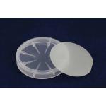
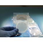
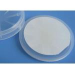
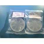
2Inch 4inch free-standing GaN Gallium Nitride Wafer |
|
5um Thickness AlN Aluminum Nitride Template 430um Sapphire 350um Sic Substrates |
|
2 4 Inch 4-5 Um III Gallium Nitride Wafer 0.43 Mm Sapphire Sic Substrates |
|
III - Nitride 2 INCH Free Standing GaN Wafer For Laser Projection Display Power Device |
|
2inch 4inch GaN-based Blue Green LED Grown On Flat Or PPS Sapphire MOCVD DSP SSP |
|
8inch GaN-on-Si Epitaxy Wafer 110 111 110 N Type P Type Customization Semiconductor RF LED |