
101 - 110 of 226
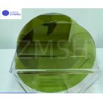
high optical transmittance substrate wafer
Selling leads
|
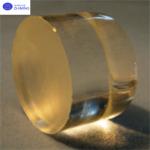
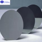
...-N SIC ingots/High purity 4H-N 4inch 6inch dia 150mm silicon carbide single crystal (sic) substrates wafers/ Customzied as-cut sic wafers ...
2025-05-06 20:41:05
|
|
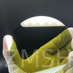
...Wafer 6inch(0001)Double Side Polished Ra≤1 nm Customization Description of 12 inch SiC wafer 4H N-type Semi-type SiC Wafer: 12 inch 6inch SiC wafer ...
2025-05-06 20:41:28
|
|
...wafer High-Frequency SAW Filters High Piezoelectric Coefficient Introduce Lithium Tantalate (LiTaO₃) is a ferroelectric crystal that has attracted ...
2025-05-29 00:09:29
|
|
... a serials of proprietary technologies and the-state-of-the art PVT growth reactors and facilities to fabricate different sizes of high-quality ...
2025-05-06 20:44:44
|
|
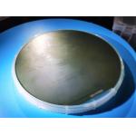
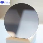
... to a silicon carbide (SiC) wafer with a 12-inch diameter (approximately 300mm), a size standard used in the semiconductor industry for the mass ...
2025-05-06 20:41:54
|
|
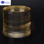
LNOI Wafer 2/3/4/6/8 Inch (Si/LiNbO₃, Customizable) photonic devices Introduce of LNOI Wafer LiNbO3 Crystals is widely used as frequency doublers for ...
2025-06-23 17:12:58
|
|
...substrate 2 4 6 inch for 2.5~25G DFB laser diode InP DFB Epiwafer InP substrate's brief InP DFB Epiwafers designed for 1390nm wavelength applicatio...
2025-05-06 20:45:38
|
|
...wafer for MOSFETs,JFETs BJTs,high resistivity wide bandgap Semi-insulating SiC substarte/wafer's abstract Semi-insulating silicon carbide (SiC) ...
2025-05-06 20:41:20
|
|
...wafer Si wafer 8inch N type P type SSP DSP Prime grade Dummy grade Product Overview: 8-Inch Prime Grade Silicon Wafer Silicon wafers are the ...
2025-05-06 20:45:52
|
|
...wafers 3inch 4inch N/P TYPE InP Semiconductor Substrate Wafers Doped S+/ Zn+ /Fe + growth (modified VFG method) is used to pull a single crystal ...
2025-05-06 20:44:36
|