
111 - 120 of 226
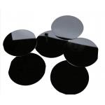
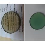
high optical transmittance substrate wafer
Selling leads
|
...wafers 3inch 4inch N/P TYPE InP Semiconductor Substrate Wafers Doped S+/ Zn+ /Fe + growth (modified VFG method) is used to pull a single crystal ...
2025-05-06 20:44:37
|

|
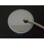
2inch 50.8mm C Miscut A 4 Degree Sapphire Wafers Thickness 0.175mm/0.3mm/0.4mm/0.5mm Dsp 2 Inch C Plane Polished Sapphire Wafers Crystal Substrates ...
2025-07-17 00:10:50
|

|
...making them highly desirable for a wide range of applications. In fact, sapphire is one of the hardest and most scratch-resistant materials ...
2025-07-17 00:10:50
|
|
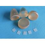
...Wafer Semiconductor Substrate For Epitaxial Growth VGF 2inch 4inch 6inch n-type prime grade GaAs wafer for epitaxial growth Gallium arsenide can be ...
2025-05-06 20:45:00
|
|
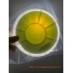
...wafers for High temperature superconducting junction technology Product Name:Strontium titanate (SrTiO 3) crystal substrateProduct Description: ...
2025-05-06 20:40:34
|
|
...wafer 1mm thickness for ingot growth Customzied size/2inch/3inch/4inch/6inch 6H-N/4H-SEMI/ 4H-N SIC ingots/High purity 4H-N 4inch 6inch dia 150mm ...
2025-05-06 20:40:57
|
|
... containing silicon and carbon with chemical formula SiC. SiC is used in semiconductor electronics devices that operate at high temperatures or ...
2025-05-06 20:40:41
|
|
2inch/3inch /4inch /6inch S-C-N Type/ semi-insulation /Si-doped Gallium arsenide GaAs Wafer Product Description Our 2’’ to 6’’ semi-conducting & semi...
2025-05-06 20:44:32
|
|
2inch/3inch /4inch /6inch S-C-N Type/ semi-insulation /Si-doped Gallium arsenide GaAs Wafer Product Description Our 2’’ to 6’’ semi-conducting & semi...
2025-05-06 20:44:52
|

|
... quality for semiconductor applications. Known for its superior optical transparency, outstanding mechanical strength, and excellent thermal ...
2025-05-06 20:40:12
|