
61 - 70 of 226
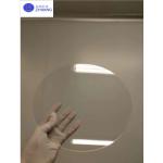
high optical transmittance substrate wafer
Selling leads
|
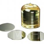
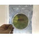
...Wafer Substrate Double or Single Polished Z-cut X-cut Y-cut Saw grade Description of LiTaO3 Wafer: Lithium tantalate (LiTaO3) has a perovskite M6 ...
2025-05-06 20:45:49
|
|
...substrate 4H-N/Semi Type SiC Ingots Industrial Dummy2inch/3inch/4inch/6inch 6H-N/4H-SEMI/ 4H-N SIC ingots/High purity 4H-N 4inch 6inch dia 150mm ...
2025-07-16 00:09:37
|
|
... The Kyropoulos process (KY process) for sapphire crystal growth is currently used by many companies in China to produce sapphire for the ...
2025-05-06 20:39:27
|
|
...substrates wafers for GaN epitaxial growth; TYPICAL CHOICES FOR PART ORIENTATION: Why Sapphire? Zero Degree: The direction of view is parallel to ...
2025-05-06 20:38:38
|
|
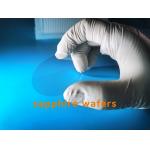
..., are valued for their high resistance to thermal shock and chemical corrosion. These wafers are commonly used in optical, electronic, and medical ...
2025-05-06 20:45:40
|
|
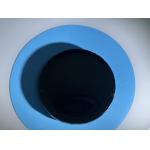
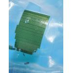
...substrates wafers, sic crystal ingots sic semiconductor substrates,Silicon Carbide crystal Wafer/ Customzied as-cut sic wafers About Silicon ...
2025-05-06 20:40:37
|
|
...wafer optical 1/2/3 inch SIC wafer for sale Sic Plate Silicon Wafer Flat Orientation Enterprises for Sale 4inch 6inch seed sic wafer 1.0mm ...
2025-07-16 00:09:36
|
|
...wafer optical 1/2/3 inch SIC wafer for sale Sic Plate Silicon Wafer Flat Orientation Enterprises for Sale 4inch 6inch seed sic wafer 1.0mm ...
2025-07-16 00:09:36
|
|
...Wafer with (111) Crystal Orientation – Introduction The 8-inch silicon wafer with (111) crystal orientation is a vital component in the semiconduct...
2025-05-06 20:45:52
|
|
...supplier of sapphire substrates for photoelectronic applications, including the high brightness LED market. The material is grown and orientated, ...
2025-07-16 00:09:37
|