
51 - 60 of 226
high optical transmittance substrate wafer
Selling leads
|
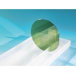
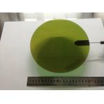
... on the market for 2 inch and 3 inch Research grade SiC substrate wafers. SiC substrate wafers have a variety of applications in electronic device ...
2025-07-17 00:10:50
|
|
...Silicon Carbide) substrate wafer, ZMSH offers the best price on the market for 2 inch and 3 inch Research grade Silicon Carbide substrate wafers. ...
2025-07-17 00:10:50
|
|
...Wafers For epitaxial Thickness 500um Double side polished DSP Special Orientation SSP/ DSP A-axis R-axis M-axis 2inch 3inch 4inch 6inch sapphire ...
2025-05-06 20:38:51
|
|
...Wafers Thickness 500UM 600um Double side polished SSP OR DSP Special Orientation SSP/ DSP A-axis R-axis M-axis 2inch 3inch 4inch 6inch sapphire ...
2025-05-06 20:38:51
|
|
... Wafer 2-8'' 4H N - Doped SiC Wafers/8inch 200mm N-type SiC Crystal Wafers Ingots SiC substrate/2inch/3inch/4inch/6inch/8inch 6H-N/4H-SEMI/ 4H-N ...
2025-05-06 20:42:04
|
|
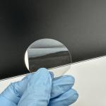
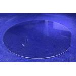
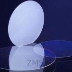
High Purity Substrate DSP/SSP Polished Sapphire Wafer Lens for sale Sapphire Optical Custom-made High Precision Transparent Sapphire Glass Optical ...
2025-05-06 20:38:05
|
|
...substrate wafer for laser device Product Type: Yttrium aluminum garnet (YAG) is an isotropic crystal with cubic symmetry. It has excellent optical ...
2025-07-17 00:10:50
|
|
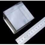
... resistant Highly chemical resistant Maximum temperature rating of almost 2000C The Detail for 2inch C-axis wafers Size: 2 inch DSP-0.1-C-Sapphire ...
2025-05-06 20:38:38
|
|
... stations powering 5G networks, and integrated into tools manufacturing next-gen microchips, quartz wafers are essential. These high-purity ...
2025-07-10 18:23:13
|
|
10x10mmt/Tellurium oxide (TeO2) crystals crystal substrate TeO2 wafer TeO2 Crystal & Q Switch TeO2 is an excellent ascousto-optic (AO) crystal with ...
2025-05-06 20:40:28
|