
11 - 20 of 226
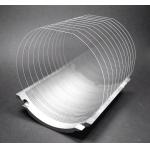
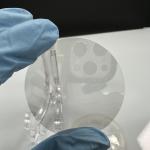
high optical transmittance substrate wafer
Selling leads
|
...:Lithium tantalate (LiTaO3) single crystal has a very good electro-optical, piezoelectric and pyroelectric properties, widely used in pyroelectric ...
2025-05-06 20:44:34
|
|
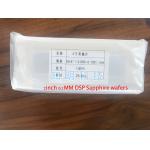
... 4inch 6inch sapphire substrates wafers for GaN epitaxial growth;0.1mm/100um 2inch sapphire c-axis substrates TYPICAL CHOICES FOR PART ORIENTATION: ...
2025-05-06 20:38:52
|
|
...substrates wafers for GaN epitaxial growth;0.1mm/100um 2inch sapphire c-axis substrates TYPICAL CHOICES FOR PART ORIENTATION: Why Sapphire? Zero ...
2025-05-06 20:38:43
|
|
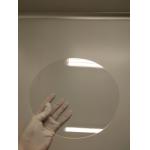
... during the range of visible and near IR spectrum.It is widely used for led substrates for GaN Epitaxial growth ;and also as optical window in ...
2025-05-06 20:40:21
|
|
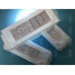
... wafers About Silicon Carbide (SiC)Crystal Silicon carbide (SiC), also known as carborundum, is a semiconductor containing silicon and carbon with ...
2025-05-06 20:42:02
|
|
...), also known as carborundum, is a semiconductor containing silicon and carbon with chemical formula SiC. SiC is used in semiconductor electronics ...
2025-05-06 20:42:00
|
|
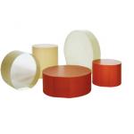
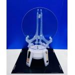
...wafer sapphire glass sapphire watch glass ar sapphire crystal sapphire wafer price 2inch 3inch 4inch 6inch 8inch 12inch 3Inch C-axis 76.2mm Al2O3 ...
2025-07-16 00:09:36
|
|
...Carbide) substrate wafers. Our wafers are optimal for electronic devices with high power and high frequency, as well as for light emitting diodes ...
2025-07-16 00:09:37
|
|
... Carrier wafers for SOS GaAs epitaxy About synthetic sapphire crystal The Kyropoulos process (KY process) for sapphire crystal growth is currently ...
2025-05-06 20:38:48
|
|
...Optical Windows SAPPHIRE WAFER WINDOW for OPTICAL LASER OPTICS APPLICATIONS High hardness Ir Optical Standard Window Multiple shapes sapphire ...
2025-07-16 00:09:37
|