
31 - 40 of 199
gan templates semiconductor substrate
Selling leads
|
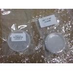
...template 8inch 6inch AlGaN/GaN HEMT-on-HR Si Epiwafer GaN-on-Si Epiwafer for Micro-LED for RF application GaN Wafer Characteristic III-Nitride(GaN...
2025-05-06 20:44:19
|
|
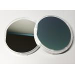
GaN-on-Si(111) N/P Ttype substrate Epitaxy 4inch 6inch 8inch for LED or Power device GaN-on-Si substrate abstract GaN-on-Si (111) substrates are ...
2025-05-06 20:45:21
|
|
... (GaN) layer on a silicon (Si) substrate, which is 8 inches in diameter. This combination leverages GaN's high electron mobility, thermal ...
2025-05-06 20:45:22
|
|
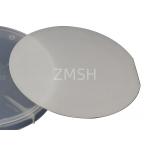
...templates 500nm AlN film on silicon substrate Applications of AlN template Silicon-based semiconductor technology has reached its limits and could ...
2025-05-06 20:44:40
|
|
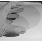
2inch 4iinch 6Inch Sapphire based AlN templates AlN film on sapphire substrate 2inch on sapphire substrate AlN Template layer Wafer For 5G BAW Devices ...
2025-05-06 20:44:44
|
|
...templates AlN film on sapphire substrate sapphire window sapphire wafer Applications of AlN template Silicon-based semiconductor technology has ...
2025-05-06 20:44:39
|
|
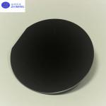
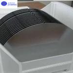
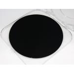
...GaN-on-Sapphire Blue/Green LED Wafer Flat or PPS Sapphire MOCVD DSP SSP Description of GaN-on-Sapphire Blue/Green LED Wafer: GaN on Sapphire (GaN...
2025-05-06 20:44:26
|
|
...GaN HEMT-on-HR Si Epiwafer GaN-on-Si Epiwafer for Micro-LED for RF application GaN Wafer Characteristic III-Nitride(GaN,AlN,InN) Gallium Nitride is ...
2025-05-06 20:44:18
|
|
... integrated at the wafer scale. The two wafers are bonded face-to-face using a low-temperature oxide-oxide bonding technique. The Si substrate of ...
2025-05-06 20:44:26
|
|
... during the range of visible and near IR spectrum.It is widely used for led substrates for GaN Epitaxial growth ;and also as optical window in ...
2025-05-06 20:40:21
|