
41 - 50 of 199
gan templates semiconductor substrate
Selling leads
|
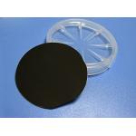
2inch R-axis sapphire wafer for epi-ready test ,sapphire optical windows, R-axis 2inch sapphire epi-ready substrate 1. Description Sapphire is one of ...
2025-05-06 20:44:14
|
|
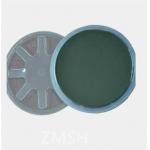
...Substrate 2inch 3inch 4inch 5inch 6inch Un/S/Zn Type N/P DSP/SSP Abstrate of Indium Arsenide (InAs) Substrates Indium Arsenide (InAs) substrates ...
2025-05-27 17:33:17
|

|
...substrate single crystal Aluminum substrate orientation 111 100 111 5×5×0.5mm a=4.040Ã single crystal Aluminum substrate's brief The demand for ...
2025-05-06 20:45:43
|
|
... to deliver optimal electrical and thermal performance for advanced semiconductor and electronic applications. These wafers are available in ...
2025-05-06 20:45:45
|
|
..., providing high-quality silicon carbide substrates that facilitate cutting-edge semiconductor research and development. 2. Product & Compony ...
2025-05-06 20:45:54
|
|
2-4inch Gallium antimonide GaSb Substrate Single Crystal Monocrystal for Semiconductor Gallium antimonide (GaSb) is a very important III-V direct ...
2025-05-06 20:44:35
|
|
...variety of applications in the telecommunications, optoelectronics, and semiconductor industries. With superior optical and electronic properties, ...
2025-05-06 20:45:10
|
|
...Wafer with (111) Crystal Orientation – Introduction The 8-inch silicon wafer with (111) crystal orientation is a vital component in the semiconduct...
2025-05-06 20:45:52
|
|
... Zinc oxide ZnO single crystal substrate Product Name: Zinc oxide (ZnO) crystal substrate Product Description: Zinc oxide (ZnO) crystal substrate ...
2025-05-06 20:40:31
|
|
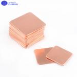
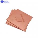
...substrate single crystal Cu wafer 5x5x0.5/lmm 10x10x0.5/1mm 20x20x0.5/1mm a=3.607A Copper substrate's abstract Our copper substrates and wafers are ...
2025-05-06 20:45:45
|