
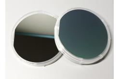
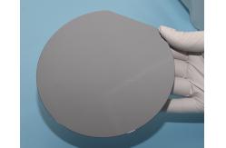
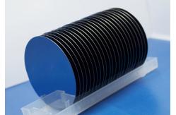
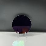
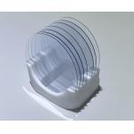
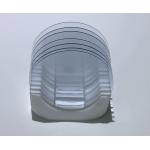
6" Silicon Based AlN Templates 500nm AlN Film On Silicon Substrate
|
Detailed Product Description
|
diameter 150mm 8inch 4inch 6inch Silicon-based AlN templates 500nm AlN film on silicon substrate
Applications of AlN template Silicon-based semiconductor technology has reached its limits and
could not satisfy the requirements of future electronic devices. As a typical kind of 3rd/4th-generation
semiconductor material, aluminum nitride (AlN) has superior physical and chemical properties such as wide bandgap,
high thermal conductivity, high breakdown filed, high electronic mobility and corrosion/radiation resistance, and is
a perfect substrate for optoelectronic devices, radio frequency (RF) devices, high-power/high-frequency electronic
devices, etc.. Particularly, AlN substrate is the best candidate for UV-LED, UV detectors, UV lasers, 5G
high-power/high-frequency RF devices and 5G SAW/BAW devices, which could widely be used in environmental protection,
electronics, wireless communications, printing, biology, healthcare, military and other fields, such as UV
purification/sterilization, UV curing, photocatalysis, coun terfeit detection, high-density storage, medical phototherapy, drug
discovery, wireless and secure communication, aerospace/deep-space detection and other fields. we have developed a serials of proprietary processes and
technologies to fabricate high-quality AlN templates. At present, Our OEM is the only
company worldwide who can produce 2-6 inch AlN templates in large-scale industrial production capability with
capacity of 300,000 pieces in 2020 to meet explosive market demand from UVC-LED, 5G wireless communication, UV detectors
and sensors etc The factroy is an innovative high-tech company founded in
2016 by renowned Chinese Overseas professionals from
semiconductor industry. they focus its core business on development and
commercialization of 3rd/4th-generation ultra-wide bandgap
semiconductor AlN substrates, AlN templates, fully automatic PVT growth reactors and related
products and services for various high-tech industries. it has been recognized as a global leader in this field. Our
core products are key strategy materials listed in “Made in
China ". they have developed a serials of proprietary
technologies and the-state-of-the art PVT growth reactors and
facilities to fabricate different sizes of high-quality single crystalline AlN
wafers, AlN temlpates. We are one of the few world-leading high-tech companies who own full AlN fabrication capa bilities to produce high-quality AlN boules and wafers, and provide
professional services and turn-key solutions to our customers, arranged from the growth reactor and hotzone design, modeling and
simulation, process design and optimization, crystal growth, wafering and material characterization. Up to April 2019, they
have applied more than 27 patents (including PCT).
Specification Characteristic Specification
|
||||||||||||||||||||
| Product Tags: AlN film on silicon substrate 500nm AlN templates 6" AlN templates |
Related Products
|
Semi Insulating GaN-On-Silicon Wafer Free Standing Gallium Nitride Substrates |
|
1inch 2inch Beta Coefficient Ga2O3 Gallium Oxide Wafer Substrate Dsp Ssp |
|
Beta Coefficient-Ga2O3 Gallium Oxide Wafer Doped Mg Fe3+ Square Substrate Dsp Ssp |

|
Large Thickness SiO2 Thermal Oxide On Silicon Wafers For Optical Communication System |
|
Y-42 Degree 4inch Lithium Tantalate LiTaO3 LiNbO3 Lithium Niobate Crystal Raw Unprocessed Ingots |

|
Single Crystal InP Indium Phosphide Wafers 350 - 650um Thickness |
Email to this supplier