
31 - 40 of 203
gallium oxide semiconductor substrate
Selling leads
|
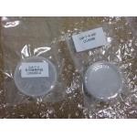
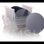
...,AlN,InN) Gallium Nitride is one kind of wide-gap compound semiconductors. Gallium Nitride (GaN) substrate is a high-quality single-crystal ...
2025-05-06 20:44:19
|
|
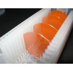
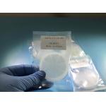
...-yellow semitransparent crystal material with an indirect band gap of 2.26 eV (300K), which is synthesized from 6N 7N high purity gallium and ...
2025-05-06 20:45:06
|
|
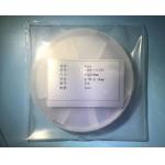
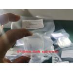
...6inch S-C-N Type/ semi-insulation /Si-doped Gallium arsenide GaAs Wafer Product Description Our 2’’ to 6’’ semi-conducting & semi-insulating GaAs ...
2025-05-06 20:44:32
|

|
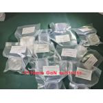
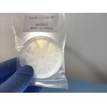
...substrates template,GaN wafer for LeD,semiconducting Gallium Nitride Wafer for ld,GaN template, mocvd GaN Wafer,Free-standing GaN Substrates by ...
2025-05-06 20:44:12
|
|
...substrates template,GaN wafer for LeD,semiconducting Gallium Nitride Wafer for ld,GaN template, mocvd GaN Wafer,Free-standing GaN Substrates by ...
2025-05-06 20:44:21
|
|
...) are 3D integrated at the wafer scale. The two wafers are bonded face-to-face using a low-temperature oxide-oxide bonding technique. The Si ...
2025-05-06 20:44:26
|
|
...substrates AlN Wafer Characteristic III-Nitride(GaN,AlN,InN) 2inch AlN template on sapphire or sic substrates, HVPE Gallium Nitride wafer,AlN ...
2025-05-06 20:44:29
|
|
...substrates template,GaN wafer for LeD,semiconducting Gallium Nitride Wafer for ld,GaN template, mocvd GaN Wafer,Free-standing GaN Substrates by ...
2025-05-06 20:44:16
|
|
..., mocvd Gallium Nitride wafer 10x10mm,5x5mm, 10x5mm GaN wafer,Non-Polar Freestanding GaN Substrates(a-plane and m-plane) 4inch 2inch free-standing ...
2025-05-06 20:44:19
|
|
... (GaN) layer on a silicon (Si) substrate, which is 8 inches in diameter. This combination leverages GaN's high electron mobility, thermal ...
2025-05-06 20:45:22
|