
41 - 50 of 203
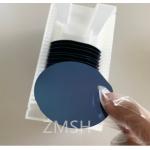
gallium oxide semiconductor substrate
Selling leads
|
...substrates template,GaN wafer for LeD,semiconducting Gallium Nitride Wafer for ld,GaN template, mocvd GaN Wafer,Free-standing GaN Substrates by ...
2025-05-06 20:44:30
|
|
...coated with a thin layer of fluorine-doped tin oxide, offering excellent electrical conductivity and optical properties. It is commonly used in ...
2025-05-06 20:45:57
|
|
...t combines high optical transparency with excellent electrical conductivity. Typically composed of indium oxide (In₂O₃) doped with tin oxide (SnO₂)...
2025-05-06 20:45:57
|
|
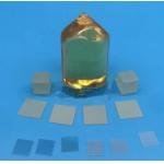
10x10mmt Terbium gallium garnet (TGG)crystals substrate wafer for laser device Product Type: Terbium gallium garnet (TGG) crystal substrateProduct ...
2025-05-06 20:40:28
|
|
.... Featuring a thickness ranging from 10μm to 25μm, this crucial substrate is available in 6-inch and 8-inch diameters, ensuring versatility for ...
2025-05-06 20:45:05
|
|
...Substrate for Epitaxy customized Abstract of SrLaAlO₄ / LaSrAlO₄/LASO SrLaAlO₄ , also written as LaSrAlO₄ depending on the elemental order, is a ...
2025-05-27 17:33:28
|
|
MgO Wafer (111) (100) Polished Magnesium oxide Monocrystal Semiconductor Customized *, *::before, *::after {box-sizing: border-box;}* {margin: 0;}html...
2025-05-06 20:45:34
|
|
...5mmt Sapphire Carrier Substrate Wafer SSP DSP Product Description: Sapphire bonding sheet is used for thinning and polishing of gallium arsenide ...
2025-07-23 00:09:03
|

|
SapphiLarge Thickness Thermal Oxide (SiO2) On Silicon Wafers For Optical Communication System Generally, the oxide layer thickness of silicon wafers ...
2025-07-23 00:09:03
|
|
2inch R-axis sapphire wafer for epi-ready test ,sapphire optical windows, R-axis 2inch sapphire epi-ready substrate 1. Description Sapphire is one of ...
2025-05-06 20:44:14
|