
11 - 20 of 203
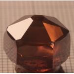
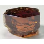
gallium oxide semiconductor substrate
Selling leads
|
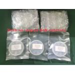
2inch InP wafers 3inch 4inch N/P TYPE InP Semiconductor Substrate Wafers Doped S+/ Zn+ /Fe + growth (modified VFG method) is used to pull a single ...
2025-05-06 20:44:36
|
|
2inch InP wafers 3inch 4inch N/P TYPE InP Semiconductor Substrate Wafers Doped S+/ Zn+ /Fe + growth (modified VFG method) is used to pull a single ...
2025-05-06 20:44:37
|
|
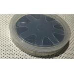
2inch 4inch 4" 2'' Sapphire based GaN templates GaN film on the sapphire substrate GaN-On-Sapphire GaN wafers GaN substrates GaN windows Properties of ...
2025-05-06 20:44:20
|
|
... on silicon substrate Applications of AlN template Silicon-based semiconductor technology has reached its limits and could not satisfy the ...
2025-05-06 20:44:38
|
|
...film on silicon substrate Applications of AlN template Silicon-based semiconductor technology has reached its limits and could not satisfy the ...
2025-05-06 20:44:41
|
|
...AlN substrate AlN single crystal wafers Applications of AlN template Silicon-based semiconductor technology has reached its limits and could not ...
2025-05-06 20:44:41
|
|
...substrate Ge window for infrared Co2 lasers Ge Material Introduce Among optical materials, germanium materials are increasingly widely used in ...
2025-05-06 20:44:48
|
|
4inch diameter 100mm Lithium niobate LiNbO3 substrate wafer, LN wafer for saw and optical,SAW Grade LiNbO3 Crystal ingot Description: Lithium niobate ...
2025-05-06 20:44:35
|
|
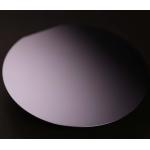
2INCH dia50.8mm Ga doped Ge substrate 4inch N-type 500um Ge wafers Ge wafer for microelectronic application N type, Sb doped Ge wafer N type,undoped ...
2025-05-06 20:44:46
|
|
2inch 4inch 4" Sapphire based GaN templates GaN film on sapphire substrate Properties of GaN Chemical properties of GaN 1) At room temperature, GaN is ...
2025-05-06 20:44:40
|