
1 - 10 of 17
gaas based epi wafer
Selling leads
|
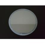
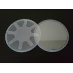
GaAs Based Epi Wafer We provides MBE / MOCVD epitaxial growth of custom structure on GaAs substrate for microelectronics , optoelectronics and RF ...
2024-12-09 13:28:02
|
|
|
GaAs Based Epi Wafer We provides MBE / MOCVD epitaxial growth of custom structure on GaAs substrate for microelectronics , optoelectronics and RF ...
2024-12-09 19:40:24
|
|
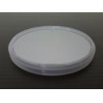
InP Based Epi Wafer We provides MBE / MOCVD epitaxial growth of custom structure on InP substrate for microelectronics , optoelectronics and RF ...
2024-12-09 13:28:02
|
|
|
InP Based Epi Wafer We provides MBE / MOCVD epitaxial growth of custom structure on InP substrate for microelectronics , optoelectronics and RF ...
2024-12-09 19:40:24
|
|
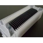
...GaAs wafer ( Gallium Arsenide ) for making LD , LED , microwave circuit, solar cell We provides both single crystal and polycrystalline GaAs wafer ...
2024-12-09 13:28:02
|
|
|
...GaAs wafer ( Gallium Arsenide ) for making LD , LED , microwave circuit, solar cell We provides both single crystal and polycrystalline GaAs wafer ...
2024-12-09 19:40:24
|
|
... material , with unique electrical properties and excellent thermal properties , compared to silicon wafer and GaAs wafer , SiC wafer is more ...
2025-04-23 07:32:19
|
|
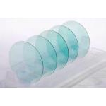
...wafer ( Gallium Antimonide ) We provides GaSb wafer ( Gallium Antimonide ) to optoelectronics industry in diameter up to 2 inch . GaSb crystal is a ...
2024-12-09 13:28:02
|
|
... cm -3 . InAs crystal has high uniformity of electrical parameters and low defect density , suitable for MBE or MOCVD epitaxial growth . We have ...
2024-12-09 13:28:02
|
|
|
... cm -3 . InAs crystal has high uniformity of electrical parameters and low defect density , suitable for MBE or MOCVD epitaxial growth . We have ...
2024-12-09 19:40:24
|