
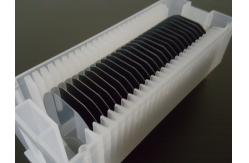
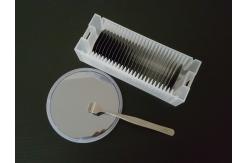
2 inch InAs Wafer Indium Arsenide one / two sides polished
|
|
InAs wafer ( Indium Arsenide )
We provides InAs wafer ( Indium Arsenide ) to optoelectronics industry in diameter up to 2 inch . InAs crystal is a compound formed by 6N pure In and As element and is grown by Liquid Encapsulated Czochralski ( LEC ) method with EPD < 15000 cm -3 . InAs crystal has high uniformity of electrical parameters and low defect density , suitable for MBE or MOCVD epitaxial growth . We have "epi ready " InAs products with wide choice in exact or off orientation , low or high doped concentration and surface finish . Please contact us for more product information .
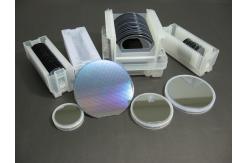
III-V Compound Wafer We provides a wide range of compound wafer including GaAs wafer, GaP wafer, GaSb wafer, InAs wafer, and InP wafer .
Electrical and Doping Specification Product Specification
|
||||||||||||||||||||||
| Product Tags: InAs Wafer Indium Arsenide 2 Inch InAs Wafer 2 Inch Indium Arsenide |

|
High Hardness High Temperature Resistance Chemical Corrosion Resistance Ceramic Arm for Semiconductor Equipment |
|
Precision Ceramic Wafer Handling Arm Aluminum Oxide |
|
Corseed Electrically Conductive Ceramics Handling Arm |

|
Thin-Film Technology |

|
DPC technology (Direct Plated Copper) |

|
Microwave Ceramic Substrates (With High Dielectric Constant) |