
DPC technology (Direct Plated Copper)
|

|
DPC technology (Direct Plated Copper)
Stapes of the technological process:
1. Formation of a thin continuous film of conductive material on a ceramic substrate. In this case, there may be holes in the substrate;
2. Applying a photoresist to the formed conductive layer;
3. Exposure and manifestation of photoresist;
4. Galvanic build-up of copper metallization of the required thickness;
5. Application of Ni-Au finish coating;
6. Removing the photoresist from the surface of the board;
7. Chemical etching of the conductive layer remaining on the ceramic after removing the photoresist.
Specifications
Technology comparance (the 5 - the best items, the 1 - the lowest items)
An equally important characteristic that determines the durability of products is the resistance of the metallized board to temperature effects. Thermal cycling testing was carried out according to MIL-STD-202.107G. This method is designed to determine the stability of a ceramic substrate with metallization to a cyclic temperature change. Test conditions:
Test results
Application area
|
|||||||||||||||||||||||||||||||||||||||||||||||||||||||||||||||||||||||||||||||||||||||||||||||||
| Product Tags: Direct Plated Copper ceramic parts DPC technology ceramic components Technical ceramic parts with DPC | |||||||||||||||||||||||||||||||||||||||||||||||||||||||||||||||||||||||||||||||||||||||||||||||||

|
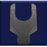
High Hardness High Temperature Resistance Chemical Corrosion Resistance Ceramic Arm for Semiconductor Equipment |
|
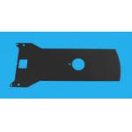
Precision Ceramic Wafer Handling Arm Aluminum Oxide |
|
Corseed Electrically Conductive Ceramics Handling Arm |

|
Ceramic Boats, Trays, And Capsules |
|
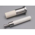
A—Two Piece Ceramic Pump |

|
Two Piece Ceramic Pump |