
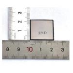
3 Inch 625um Technical Ceramic Parts GaSb Wafer Gallium Antimonide
|
|
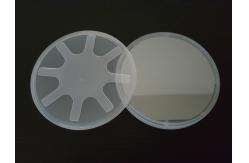
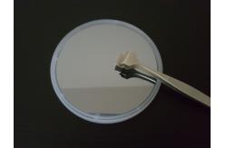
GaSb wafer ( Gallium Antimonide )
We provides GaSb wafer ( Gallium Antimonide ) to optoelectronics industry in diameter up to 2 inch . GaSb crystal is a compound formed by 6N pure Ga and Sb element and is grown by Liquid Encapsulated Czochralski ( LEC ) method with EPD < 1000 cm -3 . GaSb crystal has high uniformity of electrical parameters and low defect density , suitable for MBE or MOCVD epitaxial growth . We have "epi ready " GaSb products with wide choice in exact or off orientation , low or high doped concentration and good surface finish . Please contact us for more product information .
III-V Compound Wafer We provides a wide range of compound wafer including GaAs wafer, GaP wafer, GaSb wafer, InAs wafer, and InP wafer .
Electrical and Doping Specification
Product Specification
|
||||||||||||||||||||||
| Product Tags: Technical Ceramic Parts GaSb Wafer 3 Inch GaSb Wafer 625um Gallium Antimonide |
|
High Concentration Quantum Grade Diamond Customized Size |
|
Single Crystal Diamond Cutting Tools Good Wear Resistance |
|
Indusatial Ceramics Parts Cultured Diamonds Pink Blue Yellow |
|
Diamond Heat Dissipation Material Thermal Management For Electronic Packaging Heat Dissipation |
|
Corseed Electrically Conductive Ceramics Handling Arm |
|
High Performance Nozzle Or Injector Technical Ceramic Parts |