
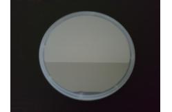
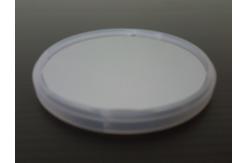
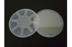
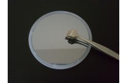
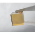
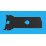
500Um To 625Um GaAs Based Epi Wafer Polished Grade mechanical grade
|
|
GaAs Based Epi Wafer
We provides MBE / MOCVD epitaxial growth of custom structure on GaAs substrate for microelectronics , optoelectronics and RF Microwave applications , in diameter Ø 3" to Ø 4” . With our extensive MOCVD experience , we can grow binary alloy ( LT-GaAs , AlAs ) or ternary alloy ( AlGaAs , InGaAs ,GaAsP , InGaP ) on GaAs substrate , singel layer or multiple-layer superlattice structures with superior crystalline quality to meet a variety of device needs . Our highly skilled experts can work with you to design and optimize your GaAs epi layer structure . Please contact us for more product information or discuss your epi layer structure . GaAs Based Epi Wafer CapabilityOur reactors are configured for a variety of material systems and
process conditions. We can provide custom epitaxy for a variety of
device applications ranging from LEDs to HEMTs .
Optoelectronic applications: Photodetectors, VCSELs, laser diodes, LEDs, SOAs, Waveguides. Electronic applications: FETs, HBTs, HEMTs, diodes, Microwave devices.
Epi Layer Structure ( HEMT / HBT )
|
|||||||||||||||||||||||||||||||||||||||||
| Product Tags: GaAs Based Epi Wafer 625Um Epi Wafer Polished Grade epiwafer |
|
High Concentration Quantum Grade Diamond Customized Size |
|
Single Crystal Diamond Cutting Tools Good Wear Resistance |
|
Indusatial Ceramics Parts Cultured Diamonds Pink Blue Yellow |
|
Diamond Heat Dissipation Material Thermal Management For Electronic Packaging Heat Dissipation |
|
Corseed Electrically Conductive Ceramics Handling Arm |
|
High Performance Nozzle Or Injector Technical Ceramic Parts |