
Single Crystal Polycrystalline GaAs Wafer Gallium Arsenide For LD LED Microwave Circuit
|
|
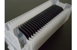
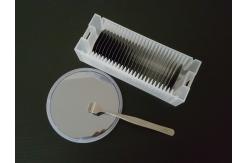
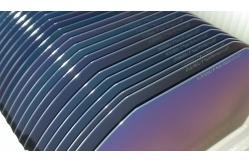
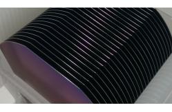
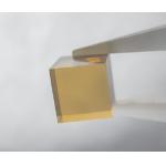
Single crystal and polycrystalline GaAs wafer ( Gallium Arsenide ) for making LD , LED , microwave circuit, solar cell
We provides both single crystal and polycrystalline GaAs wafer ( Gallium Arsenide ) to opto-electronics and micro-electronics industry for making LD , LED , microwave circuit and solar cell applications , in diameter range from 2" to 4 ". We offer single crystal GaAs wafer produced by two main growth techniques LEC and VGF method , allowing us to provide customers the widest choice of GaAs material with high uniformity of electrical propertirs and excellent surface quality . Gallium Arsenide can be supplied as ingots and polished wafers , both conducting and semi-insulating GaAs wafer , mechanical grade and epi ready grade are all available . We can offer GaAs wafer with low EPD value and high surface quality suitable for your MOCVD and MBE applications , please contact us for more product information .
GaAs Wafer Feature and Application
Product Specification
|
||||||||||||||||||||||||||||||||||
| Product Tags: Polycrystalline GaAs Wafer Single Crystal Gallium Arsenide Gallium Arsenide For LD LED |
|
High Concentration Quantum Grade Diamond Customized Size |
|
Single Crystal Diamond Cutting Tools Good Wear Resistance |
|
Indusatial Ceramics Parts Cultured Diamonds Pink Blue Yellow |
|
Diamond Heat Dissipation Material Thermal Management For Electronic Packaging Heat Dissipation |
|
Corseed Electrically Conductive Ceramics Handling Arm |
|
High Performance Nozzle Or Injector Technical Ceramic Parts |