
1 - 10 of 12
stack via sip package substrate
Selling leads
|
... with a system or sub-system in one single package. It is essential to next-generation package for fulfilling high performance and significant ...
2024-12-09 20:55:08
|
|
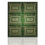
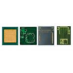
Application:Semiconductor,IC package,IC substrate,wearable electronics,IC assembly,Storage IC substrage; Spec.of Substrate production: Mini.Line space...
2024-12-09 19:38:04
|
|
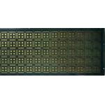
Application:Sip package substrate,Semiconductor package; Spec.of substrate production: Mini.Line space/width:1mil (25um) Finished thickness:BT (0.1-0...
2024-12-09 19:57:48
|

|
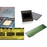
Application:Wearable electronics/Memory/DSP/ASIC/CPU/IoT industry; Spec.of Substrate production: Mini.Line space/width:1mil (25um) Finished thickness...
2024-12-09 19:38:04
|
|
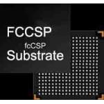
Application: FCBGA package, FCCSP package, NandFlash memory substrate,Semi Package,Semiconductors ,Semiconductor,IC package,IC substrate,uMCP,MCP,UFS...
2024-12-09 22:05:34
|
|
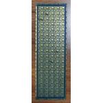
Application:Semi Package,Semiconductors ,Semiconductor,IC package,IC substrate,uMCP,MCP,UFS,CMOS,MEMS,IC assembly,Storage IC substrage;Smart phone -...
2024-12-09 19:45:11
|
|
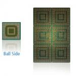
...Applicable up to 35µm pitch for flip-chip assembly (peripheral) Thin build-up laminate for SiP applications (0.3mmt for 1-2-1) Applicable ...
2024-12-09 20:55:08
|
|
...package substrate production supporting Application:IC assembly,Mobile phone,Smart phone,Digital camera electronics,Semiconductor package,IC ...
2024-12-09 20:55:08
|
|
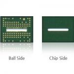
... slot. It has the bonding and solder side of the substrate in one plane. It replaced the previous lead frame into laminated substrate, which ...
2024-12-09 20:55:08
|
|
... slot. It has the bonding and solder side of the substrate in one plane. It replaced the previous lead frame into laminated substrate, which ...
2024-12-09 21:20:17
|