
51 - 60 of 79
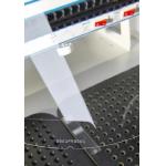
semiconductor wafer uv lithography
Selling leads
|
...Wafer with Superior Thermal and Optical Properties semiconductor and optical industries. Crafted from the purest quartz minerals, our wafers boast ...
2025-07-26 00:13:55
|
|
...renowned for its exceptional physical and optical properties, forms the cornerstone of our state-of-the-art wafers, designed to meet the most ...
2025-07-26 00:13:55
|
|
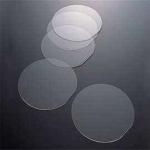
... crystal, these wafers represent the epitome of precision and purity. With their unparalleled hardness and optical clarity, Sapphire Wafers excel ...
2024-12-10 00:31:18
|
|
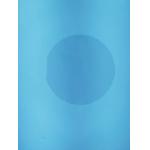
...Wafers The Ideal Material for High-Temperature Processes and Beyond Alkaline-Free Glass Wafers, a revolutionary advancement in material science ...
2025-03-06 16:31:04
|
|
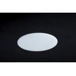
... component must meet the strictest standards. That's where our Fused Silica Wafers shine, offering a level of quality and performance that sets ...
2025-06-28 00:24:28
|
|
...Wafers The Innovative and High-Performance Choice for Your Applications Available in Multiple Sizes Are you in pursuit of the ideal substrate for ...
2025-06-28 00:24:28
|
|
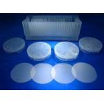
C Plane High Smoothness And High Cleanliness Sapphire Substrate For Semiconductor Sapphire wafers are mainly suitable for the research and development ...
2024-12-09 21:35:54
|
|
Semiconductor Use Fused Quartz JGS2 With Excellent Optical And Thermal Properties Fused quartz JGS2 is a type of high-purity, synthetic quartz glass ...
2024-12-09 22:13:23
|
|
...% @185nm, >90% from 200nmto 2000nm). The most seen brand/grade is JGS1, Corning 7980 and SK1300. There are also IR grade Fused Silica wafers with
2024-12-09 20:34:25
|
|
... range (>85% @185nm, >90% from 200nmto 2000nm). The most seen brand/grade is JGS1, Corning 7980 and SK1300. BonTek supply these wafers with ...
2025-07-26 00:13:55
|