
71 - 79 of 79
semiconductor wafer uv lithography
Selling leads
|
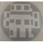
Revolutionizing Chip Fabrication Precision Innovation and Excellence At the forefront of advanced chip foundry services, we empower innovation by ...
2025-04-21 22:24:41
|
|
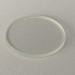
6 inch 0.5mm Borofloat 33 Glass Substrate for Semiconductor Industry and MEMS With its unique physical and chemical properties, BOROFLOAT33 has become ...
2024-12-09 20:34:25
|
|
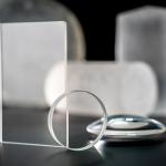
Calcium Fluoride Wafer Infrared Optics Window For a Range Of Laser, IR And UV Applications Calcium Fluoride (CaF2) has good mechanical strength and ...
2024-12-09 20:34:25
|
|
High Purity ZnO Crystal Substrate for UV Optoelectronics and Energy Harvesting Solutions Discover the remarkable qualities of ZnO Crystal, a versatile ...
2025-03-06 16:31:06
|
|
Borofloat 33 Glass Substrate for High-Temperature Applications and Precision Operations The Epitome of Precision & Durability in Glass Solutions ...
2024-12-10 00:16:16
|
|
...wafers are the epitome of modern semiconductor technology, renowned for their exceptional hardness, chemical stability, and optical transparency. ...
2024-12-09 21:17:37
|
|
ZnO Crystal Substrate Ideal Material for High Temperature/High Energy Electronic Devices and Future Wireless Communication our state-of-the-art ZnO ...
2024-12-10 00:44:27
|
|
Borofloat 33 Glass Substrate for High-Temperature Applications and Precision Operations The Epitome of Precision Durability in Glass Solutions ...
2025-03-06 16:31:01
|
|
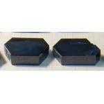
High Durability Sapphire Crystal Optics For Short And Long Wavelength Applications Sapphire is used for short and long wavelength applications (UV and ...
2024-12-09 20:34:25
|