
31 - 40 of 79
semiconductor wafer uv lithography
Selling leads
|
... wafers this is the Kyropoulos method (abbreviated to Ky or Kr). The Kyropoulos method is a continuation of the Czochralski method (CZ) which is ...
2024-12-09 20:34:25
|
|
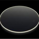
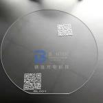
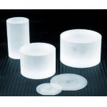
UV Grade Fused Silica Wafer 3'' 4'' 6'' JGS1 JGS2 JGS3 for Glass and Quartz Materials The Epitome of Optical Clarity and Precision Elevate your ...
2025-07-25 00:18:38
|
|
...three types of China made quartz glass, classified by their transmission range into JGS1 for UV-VIS range, JGS2 for VIS range, and JGS3 for UV-VIS...
2025-07-25 00:18:38
|
|
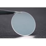
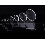
...Wafer Sapphire Wafer 330um 430um Thick Our sapphire wafers are the epitome of precision and quality, crafted from the purest sapphire crystal. ...
2024-12-09 20:34:25
|
|
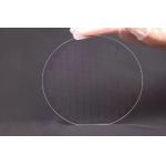
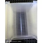
...Wafers Thickness 0.35±0.025mm in Fused Silica Borosilicate BonTek is a recognized participant in the manufacture of transparent Glass wafers. Many ...
2024-12-09 20:34:25
|
|
...Wafer for Consistent Optical Properties C-plane 0001 the Sapphire Wafer - a Unique Innovation in High-Tech Materials Step into the future with our ...
2024-12-09 23:45:42
|
|
...Wafer is a type of semiconductor material made of sapphire, which has excellent optical, mechanical, and chemical properties. It is commonly used ...
2024-12-09 23:27:58
|
|
...Wafer for Miniature Electronic Devices the Sapphire Crystal Wafer - a cutting-edge material that revolutionizes optical, electronic, and semiconduc...
2024-12-09 23:27:58
|
|
...Wafer for SAW Components Unleash the Power of Monocrystalline Quartz Wafers for Your Cutting-Edge Applications! Discover the ultimate material for ...
2025-07-25 00:18:38
|
|
... from the purest sapphire crystal, our wafers embody strength, durability, and optical excellence. Our Sapphire Wafers are renowned for their ...
2024-12-10 00:26:38
|