
41 - 50 of 79
semiconductor wafer uv lithography
Selling leads
|
Customized 6 Inch 8 Inch Piezoelectric Wafer for Semiconductor POI and MEMS Positive piezoelectric effect (direct piezoelectric effect) : The ...
2024-12-09 20:34:25
|
|
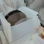
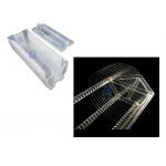
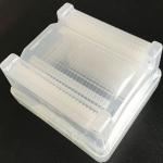
Semiconductor Cleaned Piezoelectric Wafer in stock in Class 1000 Clean Room The piezoelectric effect in a crystal is explained as that there will be ...
2025-07-25 00:18:38
|
|
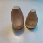
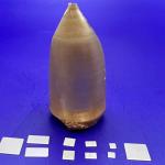
10mm Square SrTiO3 Crystal Wafer For Semiconductor SrTiO3 single crystal has the good lattice structure of perovskite structure materials. For the ...
2024-12-09 21:42:24
|
|
10mm Square Fe Doped SrTiO3 Crystal Wafer For Semiconductor Fe-doped strontium titanate (SrTiO3) and strontium titanate single crystal have similar ...
2024-12-09 21:42:24
|
|
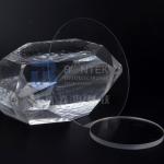
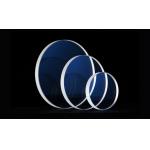
6 Inch And 8 Inch Borofloat 33 Wafer For Electronics Optics And Semiconductors Borofloat 33 Features Schott Borofloat 33 is a flat glass that sets new ...
2024-12-09 22:13:23
|
|
... in the semiconductor industries. A common application is the mechanical stabilization of thin Si-diaphragms for sensors, and etching structuring ...
2024-12-09 20:34:25
|
|
...Wafer with A-plane 11-20 Primary Flat Our sapphire wafers are precision-crafted using the finest materials and cutting-edge technology. Sapphire, a ...
2024-12-09 20:34:25
|
|
...Wafer - Perfect for demanding applications Product Description: Sapphire Wafer is a kind of sapphire plate made from high quality sapphire ...
2024-12-09 23:10:26
|
|
...Wafer with BOW 10um Product Description: Sapphire Wafer is a kind of sapphire slice that has been precision cut from a sapphire boule to the ...
2024-12-09 23:10:26
|
|
... 33 Glass Wafer for Optimal Performance in Electronics Borofloat 33 Glass Wafer Description Borofloat 33 - the ultimate choice for precision optics ...
2024-12-09 23:27:58
|