
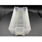
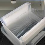
3'' to 13'' Fused Silica Wafer
|
|
3'' to 13'' Fused Silica Wafer and Fused Quartz Wafer Double Side Polish Roughness Ra 1nm
The UV grade Fused Silica wafers is made of full synthetic material with very low trace metal content, the melting method Synthetic CVD. Fused silica is highly heat resist and has a broad transmission range (>85% @185nm, >90% from 200nmto 2000nm). The most seen brand/grade is JGS1, Corning 7980 and SK1300.
There are also IR grade Fused Silica wafers with transmission from 185nm to 350nm. The IR grade fused silica is usually with very low OH content (i.e., <5ppm), the melting method electrical melting. The brand/grade for this type is JGS3, Corning 7979 and SK1310. BonTek supply these wafers with diameter up to 8’’ 200mm, Ra<0.5nm.
Fused Quartz wafers are with low OH content and relatively low trace metal content. It is of good chemical purity, very high heat resistance, the transmission is from 260nm to 2100nm. JGS2 is a kind of fused quartz often used. BonTek can provide JGS2 fused quartz wafers up to 12 inch 300mm diameter, the flatness, surface roughness, TTV, Bow, warp all in good quality.
FAQs:
A: We look at ourselves as the piezo wafer specialist. We are the very first to work with Single Crystal Quartz in China about 30 years ago. Then gradually we step in the field of LiNbO3, LiTaO3, Quartz glass, LGS, CTGS etc. Especially, if you are looking for a piezo quartz supplier, we are the ultimate choice! We export millions of quartz blanks each year because we master the AT, SC and IT cuts with superior angle precision.
A: Yes, of course. We can fabricate as per your request. In addition, we are so experienced with piezo wafers that we can provide you relevant suggestions if you are not 100% sure about your choice. Besides, we do have some standard wafers in stock, please check with us.
A: Yes, we would suggest you go with the courier agent you are most familiar with (DHL, FedEX, UPS etc.). We can ship via your account. And, of course, we will pack the products safely in acceptable size to help you save the shipping cost. If you need us to take care of the freight, it’s also not a problem. We also have good discount with the international courier companies.
A: The wafer products are fragile and sometimes expensive. The last thing, as the manufacturer, we want to see is the products we make were damaged during courier. As a result, we will pack the wafers adequately and put them in a proper carton filled with buffer sponge. However, accidents are inevitable sometimes. So, please follow the “Acceptance check” steps shown in the drawings below. If the unwanted happened, we will either give the replenishment or refund if you follow the checking steps.
A: Sure. Factory inspection is important for large quantity purchase and long-term cooperation. Face to face discussion is what we mostly confident with. During the past years, big names around the world have witnessed our progress in factory build-up. These days, due to the Covid-19 pandemic, we also had the experience of videoconferencing with global buyers.
Acceptance Check
|
|||||||||||||||||||||||||||||||||||||||||||||||||||||||||||||||||||||||||||||||||||||||||||||||||||||
| Product Tags: 13'' Fused Silica Wafer 3'' Fused quartz wafer Fused Silica Wafer Roughness Ra 1nm | |||||||||||||||||||||||||||||||||||||||||||||||||||||||||||||||||||||||||||||||||||||||||||||||||||||
|
UV Grade Fused Silica Wafer 3'' 4'' 6'' JGS1 JGS2 JGS3 for Glass and Quartz Materials |

|
B270 Glass Wafer Optical Substrates For Versatile Applications |

|
8 Inch 12 Inch JGS1 Fused Quartz Wafers For Optics Lasers And Semiconductors |
|
0.05mm To 10mm Fused Silica Wafer Quartz Wafer JGS1 JGS2 JGS3 |
|
350um Fused Silica Wafer Quartz Borosilicate Glass Carrier Wafers |

|
SiO2 Fused Quartz And Fused Silica Wafer In Infrared And Ultraviolet Spectrum |