
350um Fused Silica Wafer Quartz Borosilicate Glass Carrier Wafers
|
|
Fused Silica Quartz Borosilicate Glass Wafer As Carrier Wafers
Due to their low thickness, thin wafers are vulnerable to stress and breakage. Warping of the wafers during handling and processing causes a high yield loss or can even make it impossible to handle the wafers any more. This means that a thin wafer handling technology with a high degree of flexibility on wafer and substrate sizes is needed. Carrier wafers need to have certain properties, such as: mechanical robustness; chemical and high-temperature resistance; incredibly low tolerances (down to 1 μm thickness variation); and thermal expansion adjusted to the used material, for example, gallium arsenide (GaAs), Indium phosphide (InP), silicon (Si) or silicon carbide (SiC). Furthermore, handling tools sometimes need to be suitable for materials such as GaAs and Si, or even CMOS compatible. High-end carrier wafers made of glass, quartz or silicon can meet the aforementioned requirements. Glass and quartz are excellent materials for carrier wafers because of their thermal stability and resistance against acids and other chemicals. Bonding to and de-bonding from glass and quartz carrier wafers can be monitored since they are transparent. Furthermore, glass carrier wafers can be cleaned and re-used, thus contributing to cost reduction and environmental protection. BonTek works on a variety of glass and quartz materials, Fused Silica (JGS1, JGS2, JGS3, Corning 7980), Eagle XG, Schott BF33, Pyrex, MEMpax, B270, D263T, Zerodur etc.
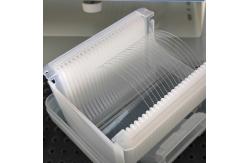
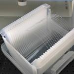
Acceptance Check
|
||||||||||||||||||||||||||||||||||||||||||||||||||||||||||||||||||||||||||||||||||||||||||||||||||||||||||||||||||||||||||||||||||||||||||||||||||||||||||||||||
| Product Tags: Fused Silica Borosilicate Glass Wafer Fused Silica Wafer 350um Fused Silica Quartz Carrier Wafer | ||||||||||||||||||||||||||||||||||||||||||||||||||||||||||||||||||||||||||||||||||||||||||||||||||||||||||||||||||||||||||||||||||||||||||||||||||||||||||||||||
|
UV Grade Fused Silica Wafer 3'' 4'' 6'' JGS1 JGS2 JGS3 for Glass and Quartz Materials |

|
B270 Glass Wafer Optical Substrates For Versatile Applications |

|
8 Inch 12 Inch JGS1 Fused Quartz Wafers For Optics Lasers And Semiconductors |
|
0.05mm To 10mm Fused Silica Wafer Quartz Wafer JGS1 JGS2 JGS3 |
|
350um Fused Silica Wafer Quartz Borosilicate Glass Carrier Wafers |

|
SiO2 Fused Quartz And Fused Silica Wafer In Infrared And Ultraviolet Spectrum |