
81 - 90 of 343
single crystal optical windows
Selling leads
|
... integrated circuits. The wafer is processed through high-temperature melting and single-crystal growth, ensuring purity and crystal integrity. ...
2025-05-06 20:41:17
|
|
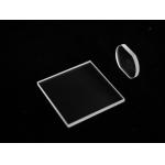
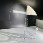
...optical plano convex lenses AR coated cylinder lenses fused silica quartz convex cylindrical lens for 2D 3D laser radar JGS1 JGS2 Product ...
2025-05-27 17:33:17
|
|
2-4inch Gallium antimonide GaSb Substrate Single Crystal Monocrystal for Semiconductor Gallium antimonide (GaSb) is a very important III-V direct ...
2025-05-06 20:44:35
|
|
... InP Semiconductor Substrate Wafers Doped S+/ Zn+ /Fe + growth (modified VFG method) is used to pull a single crystal through a boric oxide liquid ...
2025-05-06 20:44:36
|
|
10x10mm or diameter 10mm dia25.4mm dia30mm, dia45mm, dia50.8mm AlN substrate AlN single crystal wafers Applications of AlN template Silicon-based ...
2025-05-06 20:44:41
|
|
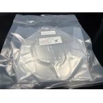
8inch Dia200mm C-Plane Al2O3 99.999% Sapphire Single Crystal Wafer Carrier Substrate 1sp 2sp *, *::before, *::after {box-sizing: border-box; } * ...
2025-07-25 00:10:23
|
|
12Inch 300mm Thickness 1.0mm Sapphire Wafers Substrate Ssp Dsp C-Plane Single Crystal 99.999% Al2O3 Sapphire wafers are known for their exceptional ...
2025-07-25 00:10:23
|
|
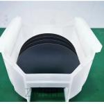
.... Silicon, a semiconductor material, is used to manufacture these wafers due to its excellent electrical properties. Silicon wafers are thin, disk...
2025-05-06 20:45:08
|
|
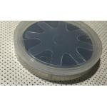
Ni Substrate single crystal cubic structure a=3.25A purity 99.99% density 8.91 Ni Substrate's abstract Nickel (Ni) substrates, particularly in the ...
2025-05-06 20:45:48
|
|
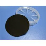
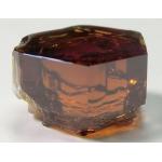
Moissanite Raw Stone Champagne Colo Silicon carbide single crystal Mohs scale 9.25 for Jewelry Industry Champagne-Colored Moissanite‘s abstract ...
2025-05-06 20:47:11
|