
Premium Silicon Wafers High Purity Single Crystal Silicon Wafers Customizable Options
|
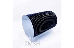
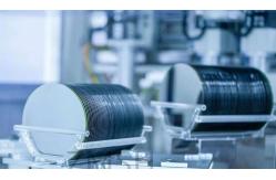
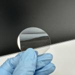
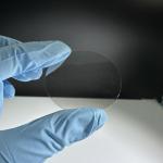
AbstractThis product is a high-purity silicon wafer, designed specifically for the manufacture of high-performance integrated circuits. The wafer is processed through high-temperature melting and single-crystal growth, ensuring purity and crystal integrity. With strict surface treatment and quality control, the product demonstrates exceptional flatness and uniformity, providing a solid foundation for micro- and nano-processing. Its low impurity content and high electron mobility make it excel in high-frequency and high-speed electronic applications. This reliable and stable high-purity silicon wafer product has been recognized and applied by numerous semiconductor manufacturing enterprises worldwide. ApplicationMicro Motors: Employed as components in micro motors, applied in precision instruments and Micro-Electro-Mechanical Systems (MEMS).
Nanotechnology: high-purity silicon wafers used for the growth and processing of nanostructures.
Biotechnology: Serves as the base material for biosensors and microfluidic chips.
High-Frequency Microwave Components: high-purity silicon wafers used in the production of high-frequency microwave components for radar, communication, and navigation systems.
Semiconductor Lasers: Acts as the substrate material for semiconductor lasers.
Photo Detectors: high-purity silicon wafers used in the manufacture of photodetectors, applied in cameras, fiber-optic communications, etc.
Microwave Devices: Utilized in the production of various microwave devices, such as oscillators and amplifiers. FeatureFast Delivery: With efficient production and logistics, we ensure timely delivery of your order, helping you maintain project timelines.
Reliable Performance: Our high-purity silicon wafers are designed to deliver reliable and consistent performance, ensuring the success of your projects.
Innovative Solutions: We constantly innovate and improve our products, staying ahead of industry trends to provide you with cutting-edge solutions.
Sustainability: Committed to sustainability, our manufacturing processes are designed to minimize environmental impact.
Stringent Testing: Each high-purity silicon wafers undergoes stringent testing to ensure it meets our high standards of quality and performance.
Global Reach: With a global network, we are well-positioned to serve customers around the world, providing local support and expertise.
Trusted Reputation: With years of industry experience, we have built a reputation for quality, reliability, and customer satisfaction.
Extensive Research and Development: Our commitment to R&D ensures continuous improvement in our products, pushing the boundaries of what's possible.
Customer-Centric Approach: We prioritize our customers, tailoring our services and solutions to meet your unique needs and expectations.
These selling points highlight the quality, reliability, and innovation associated with high-purity silicon wafers, aiming to attract and reassure potential customers.
Packing and Shipping:
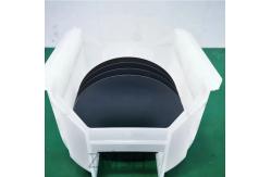
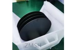
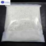
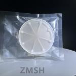
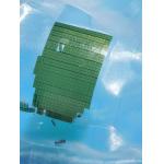
Packaging and Shipping Silicon Carbide Wafers Silicon Carbide (SiC) Wafers are thin slices of semiconductor material primarily used for power electronics. To ensure the wafers are not damaged during shipping, it’s important to follow the proper packaging and shipping instructions. Packaging
Shipping
|
||||||||||||||||||||||||||||||||
| Product Tags: Customizable Silicon Wafers High Purity Silicon Wafers Single Crystal Silicon Wafers |
|
High Purity Semi-Insulating HPSI SiC Powder/99.9999% Purity Crystal Growth |
|
Semi-Insulating SiC Wafers 3inch 76.2mm 4H Type SiC For Semiconductors |
|
High Resistivity 8inch 200mm Silicon Carbide Wafer Production Grade 4H-N |
|
4H/6H Semi-Insulating Silicon Carbide Wafer For Production/Research/Dummy Grade |
|
Square SiC Windows Silicon Carbide Substrate 1x1x0.5mmt SiC Lens |
|
Semi Insulating Silicon Carbide Wafer SiC Substrate Orientation 0001 Bow/Warp ≤50um |