
91 - 100 of 175
monocrystal semiconductor substrate
Selling leads
|
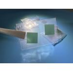
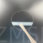
... For seed growth 6H-N/6H-Semi 4H HPSI 5*10mmt 10x10mmt 5*5mm polished Silicon Carbide sic substrate chips Wafer About Silicon Carbide (SiC)Crystal ...
2025-08-01 00:08:35
|
|
... For seed growth 6H-N/6H-Semi 4H HPSI 5*10mmt 10x10mmt 5*5mm polished Silicon Carbide sic substrate chips Wafer About Silicon Carbide (SiC)Crystal ...
2025-08-01 00:08:35
|
|
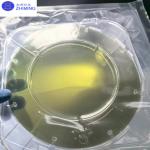
... (SiC) wafers and substrates are specialized materials used in semiconductor technology made from silicon carbide, a compound known for its high ...
2025-05-06 20:41:28
|
|
... integrated at the wafer scale. The two wafers are bonded face-to-face using a low-temperature oxide-oxide bonding technique. The Si substrate of ...
2025-05-06 20:44:26
|
|
*, *::before, *::after {box-sizing: border-box;}* {margin: 0;}html, body {height: 100%;}body {line-height: 1.5;-webkit-font-smoothing: antialiased;...
2025-08-01 00:08:35
|
|
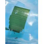
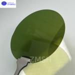
12inch SiC wafer Silicon Carbide wafer 300mm 750±25um 4H-N type orientation 100 Production Research grade 12inch SiC wafer's abstract This 12-inch ...
2025-05-06 20:41:55
|
|
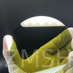
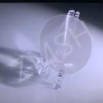
SiC Epitaxial Wafer Overview 4-inch (100 mm) SiC Epitaxial Wafers continue to play a vital role in the semiconductor market, serving as a highly ...
2025-07-10 18:23:23
|

|
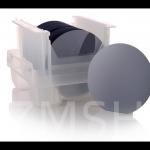
.../3 inch/4 inch 350-650 um InP Crystal Wafer Dummy Prime Semiconductor Substrate Shanghai Xinkehui New Materials Co. Ltd. We specialize in ...
2025-08-01 00:08:35
|
|
... quality for semiconductor applications. Known for its superior optical transparency, outstanding mechanical strength, and excellent thermal ...
2025-05-06 20:40:12
|
|
...semiconductor substrate primarily used in the fabrication of various electronic and optoelectronic devices. Gallium Phosphide (GaP) wafers exhibit ...
2025-05-06 20:45:06
|