
121 - 130 of 175
monocrystal semiconductor substrate
Selling leads
|
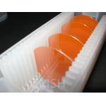
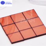
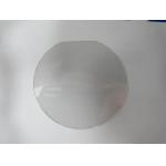
GaP Wafer, Gallium Phosphide single crystal Orientation (111)A 0°±0.2 Solar Cells Product Description: Gallium Phosphide GaP, an important semiconduct...
2025-05-06 20:45:06
|
|
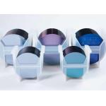
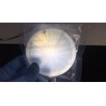
SOI wafers 4 Inches, 6 Inches, 8 Inches, Compatible with CMOS three-layer structure Product Description: The SOI (Silicon on Insulator) wafer stands ...
2025-05-06 20:45:07
|
|
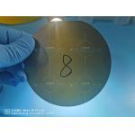
Silicon Wafer CZ orientation111 Resistivity: 1-10 (ohm.cm) single side or double side polish Product abstract Our Si wafer offers high purity and ...
2025-05-06 20:45:12
|
|
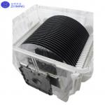
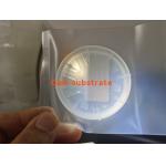
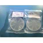
8inch si wafer CZ 200mm Prime Grade Silicon Wafer , SSP,DSP P type,B dopant,for semiconducter matrial Product Introduction: 8-Inch (200mm) Prime Grade ...
2025-05-06 20:45:53
|
|
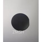
ZnTe: ZnTe wafer, ZnTe crystal Type N, Type P, Custom Sizes and Specifications Available Abstract of ZnTe Zinc telluride (ZnTe) is a direct bandgap ...
2025-05-06 20:45:56
|
|
... 6inch dia 150mm silicon carbide single crystal (sic) substrates wafers, sic crystal ingots sic semiconductor substrates,Silicon Carbide crystal ...
2025-05-06 20:40:44
|
|
...ingots/High purity 4H-N 4inch 6inch dia 150mm silicon carbide single crystal (sic) substrates wafers, sic crystal ingots sic semiconductor ...
2025-05-06 20:40:47
|
|
...substrates template,GaN wafer for LeD,semiconducting Gallium Nitride Wafer for ld,GaN template, mocvd GaN Wafer,Free-standing GaN Substrates by ...
2025-05-06 20:44:12
|
|
...substrates template,GaN wafer for LeD,semiconducting Gallium Nitride Wafer for ld,GaN template, mocvd GaN Wafer,Free-standing GaN Substrates by ...
2025-05-06 20:44:13
|
|
...substrates template,GaN wafer for LeD,semiconducting Gallium Nitride Wafer for ld,GaN template, mocvd GaN Wafer,Free-standing GaN Substrates by ...
2025-05-06 20:44:28
|