
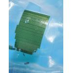
SiC Epitaxial Wafer 4H/6H SiC Substrates Custom Thickness Doping
|
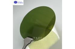
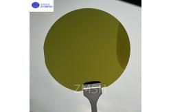
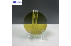
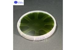
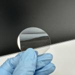
SiC Epitaxial Wafer Overview4-inch (100 mm) SiC Epitaxial Wafers continue to play a vital role in the semiconductor market, serving as a highly mature and reliable platform for power electronics and RF device manufacturers worldwide. The 4” wafer size strikes an excellent balance between performance, availability, and cost-effectiveness—making it the industry’s mainstream choice for mid-to-high volume production. SiC epitaxial wafers consist of a thin, precisely controlled layer of silicon carbide deposited on a high-quality monocrystalline SiC substrate. The epitaxial layer is engineered for uniform doping, excellent crystalline quality, and ultra-smooth surface finish. With a wide bandgap (3.2 eV), high critical electric field (~3 MV/cm), and high thermal conductivity, 4” SiC epitaxial wafers enable devices that outperform silicon in high-voltage, high-frequency, and high-temperature applications. Many industries—ranging from electric vehicles to solar energy and industrial drives—continue to rely on 4” SiC epitaxial wafers to manufacture efficient, robust, and compact power electronics.
Manufacturing PrincipleThe production of 4” SiC epitaxial wafers involves a highly controlled Chemical Vapor Deposition (CVD) process:
Specifications
Applications4” SiC epitaxial wafers enable mass production of reliable power devices in sectors including:
Frequently Asked Questions (FAQ)1. Why choose SiC epitaxial wafers over silicon?
2. What is the most common SiC polytype?
3. Can the doping profile be customized?
4. Typical lead time?
5. What quality checks are performed?
6. Are these wafers compatible with silicon fab equipment?
Related Products
12 inch SiC Wafer 300mm Silicon Carbide wafer Conductive Dummy Grade N-Type Research grade
4H/6H P-Type Sic Wafer 4inch 6inch Z Grade P Grade D Grade Off Axis 2.0°-4.0° Toward P-type Doping |
||||||||||||||||||||||||||||||||||||||||||||||||||||||||||||||||||||||||||||||||||||||||||||||||||||||||||||||||||||||||||||||||||||||||||||||||||||||||||||||||||||||||||||||||||||||||||||||||||||||||||||||||||||||||||||||||||||||||||||||
| Product Tags: Custom Thickness SiC Epitaxial Wafer Doping SiC Epitaxial Wafer 4H SiC Epitaxial Wafer | ||||||||||||||||||||||||||||||||||||||||||||||||||||||||||||||||||||||||||||||||||||||||||||||||||||||||||||||||||||||||||||||||||||||||||||||||||||||||||||||||||||||||||||||||||||||||||||||||||||||||||||||||||||||||||||||||||||||||||||||
|
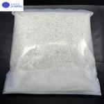
High Purity Semi-Insulating HPSI SiC Powder/99.9999% Purity Crystal Growth |
|
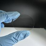
Semi-Insulating SiC Wafers 3inch 76.2mm 4H Type SiC For Semiconductors |
|
High Resistivity 8inch 200mm Silicon Carbide Wafer Production Grade 4H-N |
|
4H/6H Semi-Insulating Silicon Carbide Wafer For Production/Research/Dummy Grade |
|
Square SiC Windows Silicon Carbide Substrate 1x1x0.5mmt SiC Lens |
|
Semi Insulating Silicon Carbide Wafer SiC Substrate Orientation 0001 Bow/Warp ≤50um |