
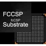
semiconductor FCCSP Package Substrate manufacture
|
|
Application:FCCSP package,IC assembly,Semiconductor package,IC package,Consumer electronics,Computer,others; Spec.of Substrate production: Mini.Line space/width:1mil (25um) Finished thickness:0.3mm; Material brand:Mainly brand:SHENGYI,Mitsubishi(BT-FR4),mitsuiseiki,OhmegaPly,Ticer,AMC,Isola,AGC,Neclo,Rogers,Taconic,Others; Surface finished:Mainly immersion gold,support customize such as OSP/Immersion silver,tin,more; Copper:10-15um or Customize; Layer:1-6 layer (Customize); Soldermask:Green or Customize (Brand:Soldermask:TAIYO INK,ABQ)
Short introduction of Horexs Manufacturer: HOREXS-Hubei is belong to HOREXS Group, is one of the leading and fast-growing Chinese IC substrate manufacturer.Which was located in Huangshi city of Hubei province China. Factory-Hubei is more than 60000 square meters floor space, which invested more than 300 million USD. IC Substrate Capacity 600,000SQM/Year,Tenting&SAP process. HOREXS-Hubei is committed to the development of IC substrate in China, striving to become one of the top three IC substrate manufacturers in China, and striving to become a world-class IC board manufacturer in the world . Technology like L/S 20/20un,10/10um.BT+ABF materials. Support: Wire bonding Substrate Wire bonding(BGA) Substrate Embedded (Memor y IC substrate) MEMS/CMOS,Module(RF,Wireless ,Bluetooth) 2/4/6L (1+2+1/2+2+2/1+4+1),Buildup(Buried/Blind hole) Flipchip CSP; Others ultra ic package substrate.
When you send inquiry us,Pls be know that we have to get the following : 1-Substrate production sepc. information; 2-Gerber files(Substrate designer/engineer can export it from your layout software,also send us drilling file) 3-Quantity request,Including sample; 4-Multilayer Substrate,please also provide us layer stack-up/Buildup information;
Process Capability
Shipping supporting: DHL/UPS/Fedex; By air; Customize express(DHL/UPS/Fedex) |
|
semiconductor FCCSP Package Substrate manufacture |
|
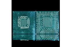
0.3mm FCCSP Package Substrate 4L Buildup Types ENEPIG 5*5mm BT Material |
|
BT FCCSP Package Substrate 3x3mm Green Color For Flip Chip Assembly |
|
BT FCCSP Package Substrate 3x3mm Green Color For Flip Chip Assembly |
|
FCCSP substrate manufacture supporting China |
|
FCCSP package substrate 4L Buildup types ENEPIG |