
51 - 60 of 79
polished silicon wafer
Selling leads
|
Z-Cut X-Cut LiNbO3 Crystals Wafer Optical Grade Both Sides Polish The sound velocity for the longitudinal waves in LiNbO3 propagating along the ...
2025-07-24 00:21:42
|
|
High Resistance Sapphire Polished Wafer 3 Inch C-Plane Optical Crystal Sapphire is a single crystal of alumina and is the second-hardest material in ...
2024-12-09 21:35:54
|
|
2 Inch 4 Inch 6 Inch Sapphire Single Crystal Wafer With Various Orientations Sizes: 2 ", 4 ", 6 "and cut small pieces; C direction, M direction, R ...
2024-12-09 21:37:23
|
|
... or wafer made from a thin layer of LiTaO3 material. Size: The thin film has a diameter of 3 inches, which is equivalent to approximately 76 ...
2025-07-24 00:21:42
|

|
... Quartz Wafer seedless or withseed SAW use BAW use Quartz used in the manufacture of frequency control products is mono-crystalline of an ...
2025-07-24 00:21:42
|
|
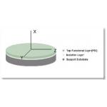
.... LNOI substrates are fabricated by transferring a thin layer of lithium niobate (LiNbO3) crystal onto an insulating substrate, typically silicon ...
2025-07-24 00:21:42
|
|
... Fused Silica Wafer 4'' 6'' 500um SiO2 HPFS with Excellent Chemical Resistance Fused Silica (SiO2) wafers are made from high purity fused silica, ...
2024-12-09 20:34:25
|
|
BonTek BT DT Cut 4 Inch Crystal Quartz Wafers All single crystal quartz wafersshould be growthn from one special seed. And the different cut type will ...
2024-12-09 21:20:33
|
|
Revolutionizing Sensing Technology: The Pyroelectric Effect in LiTaO3 Wafers Unlock the secrets of LiTaO3 and its pyroelectric effect, a phenomenon ...
2024-12-09 22:59:53
|
|
...Wafer for SAW use Crystallographic Orientation Although with the same chemical composition is silicon dioxide (SiO2), Crystal quartz, is different ...
2025-07-24 00:21:42
|