
21 - 30 of 79
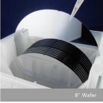
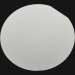
polished silicon wafer
Selling leads
|
... are three common shapes of quartz wafers: round, square, or rod type (also square, but relatively small). When the orientation is different, its ...
2024-12-09 20:34:25
|
|
... in the VIS and UV is approx. The transmission range of significantly cheaper JGS2 wafers is shifted towards longer wavelengths when compared with ...
2024-12-09 20:34:25
|
|
...common shapes of quartz wafers: round, square, or rod type (also square, but relatively small). When the orientation is different, its piezoelectri...
2025-07-24 00:21:42
|
|
...Polished Single Crystal Quartz Wafer for SAW Components Unleash the Power of Monocrystalline Quartz Wafers for Your Cutting-Edge Applications! ...
2025-07-24 00:21:42
|
|
6'' 0.5mm Single Side Polish LiTaO3 Wafer for Nonlinear Optics, Passive Infrared Sensors The LiTaO3 Lithium Tantalate crystal has >99.99% purity. Find ...
2024-12-09 20:34:25
|
|
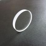
Product Description: Fused Silica Wafer is a high-performance, cost-effective IC Silicon Wafer product that is widely used in the semiconductor, MEMS ...
2024-12-09 22:58:07
|
|
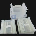
...an ideal material for Anodic bonding. BonTek provides borosilicate wafers from 2 to 14 inches diameter, the thickness is 100um up with low ...
2024-12-09 20:34:25
|
|
... and the reverse effect can also happen. Piezoelectric materials have non-conductive nature and they can be classified as ceramics and crystals. ...
2024-12-09 20:34:25
|
|
... stress, an electric field or charge proportional to the stress will be generated. This phenomenon is called the positive piezoelectric effect. ...
2024-12-09 20:57:43
|
|
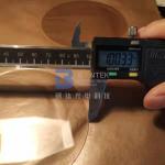
.... It has an orientation of ±0.5°, a wafer shape, a clear aperture of greater than 90%, and TTV of ≤3μm. It is also customizable in size to meet the ...
2024-12-09 23:10:26
|