
11 - 20 of 79
polished silicon wafer
Selling leads
|
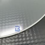
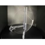
Various Type of Glass Wafers Used In Semiconductor, Optical, Medical, Military, Photonic Industry BonTek can make transparent glass wafers from any ...
2025-07-24 00:21:42
|
|
... or wafer made from a thin layer of LiNbO3 material. Size: The thin film has a diameter of 3 inches, which is equivalent to approximately 76 ...
2024-12-09 22:36:19
|
|
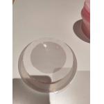
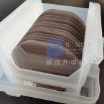
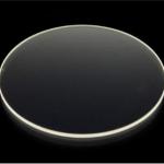
...Wafer and BF33 C7980 BK7 H-K9L Glass Wafers The glass wafers are widely used as bonding material with silicon wafers in semiconductor industry. ...
2024-12-09 20:34:25
|
|
..., and a wide transparency range going from ultraviolet to infrared. It is desirable that LiTaO3 wafer was a smooth surface in order to function ...
2025-07-24 00:21:42
|
|
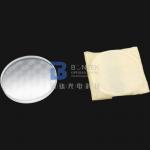
.... Such wafers are most commonly specified as 3" diameter with a reference flat. Wafer orientation is customer specified based on desired component ...
2025-07-24 00:21:42
|
|
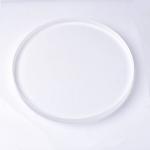
.... Fused Silica Wafer has very low thermal expansion coefficient, excellent electrical insulation properties, and superior thermal shock resistance. ...
2024-12-09 22:58:07
|
|
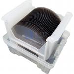
4 Inch Double Side Polish LiNbO3 Wafer 128Y Cut For SAW Filters Transducers Lithium Niobate is a ferroelectric material suitable for a variety of ...
2025-07-24 00:21:42
|
|
4 Inch 0.5mm Double Side Polish LiNbO3 Wafer 128Y Cut For SAW Filters Transducers Lithium Niobate is a ferroelectric material suitable for a variety ...
2024-12-09 20:34:25
|
|
...Wafer Polished 0.25mol% Er Dope Or 5mol% MgO Dope For Optical Applications Doped LN Wafers: Er:LN, MgO:LN, and Fe:LN Doping lithium niobate (LN) ...
2025-07-24 00:21:42
|
|
... wafers this is the Kyropoulos method (abbreviated to Ky or Kr). The Kyropoulos method is a continuation of the Czochralski method (CZ) which is ...
2024-12-09 20:34:25
|