
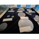
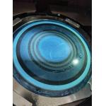
4 Inch LNOI Wafer Achieving Compact Photonic Integration
|
|
Achieving Compact Photonic Integration With 4-Inch LNOI Wafers
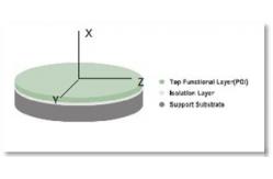
LNOI stands for Lithium Niobate on Insulator, which is a specialized substrate technology used in the field of integrated photonics. LNOI substrates are fabricated by transferring a thin layer of lithium niobate (LiNbO3) crystal onto an insulating substrate, typically silicon dioxide (SiO2) or silicon nitride (Si3N4). This technology offers unique advantages for the development of compact and high-performance photonic devices.
The fabrication of LNOI substrates involves bonding a thin layer of LiNbO3 onto an insulating layer using techniques like wafer bonding or ion-cutting. This results in a structure where LiNbO3 is suspended on a non-conductive substrate, providing electrical isolation and reducing the optical waveguide losses.
Applications of LNOI:
|
||||||||||||||||||||||||||||||||||||||||||||||||||||||||||||||||||||||||||||
| Product Tags: LNOI Piezoelectric Wafer 4 Inch LNOI Wafer 300nm LiNbO3 On Insulator | ||||||||||||||||||||||||||||||||||||||||||||||||||||||||||||||||||||||||||||
|
Stoichiometric LiTaO3 Wafers Ideal Material for Optical Modulators and Frequency Converters |
|
3" 4" 6" Single Crystal Quartz With Customized Wafers And Their Outstanding Material Properties |
|
3" 4" 6"Single Crystal Quartz Wafers For High Temperature Applications Customized Orientation Options With 3 Inch And 4 Inch Sizes |
|
3 Inch And 4 InchCustomized Orientation Options For Single Crystal Quartz Wafer High Temperature |
|
Stoichiometric LiTaO3 Wafers The Ultimate Choice for High-Frequency Electronics |
|
2" 3" 4" 6" Lithium Tantalate Wafers Ultimate Solution For Piezoelectric Applications |