
1 - 10 of 36
idt use 8 inch wafer
Selling leads
|
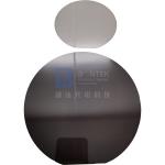
...Inch 128Y-cut Black LiNbO3 Wafer SAW Application IDT use Ra Roughness 1nm The reduction technology is used to produce Black Lithium Niobate (LiNbO3...
2024-12-09 20:34:25
|
|
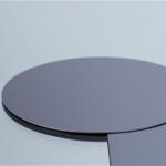
...Wafer 8 Inch 128Y-cut SAW IDT Application Lithium Niobate (LiNbO3) is a ferroelectric material suitable for a variety of applications. Its ...
2025-08-03 00:13:22
|
|
...Wafer 8 Inch 128Y-cut SAW IDT Application Lithium Niobate (LiNbO3) is a ferroelectric material suitable for a variety of applications. Its ...
2024-12-09 20:34:25
|
|
...Wafer SAW Application IDT use Ra Roughness 1nm The reduction technology is used to produce Black Lithium Niobate (LiNbO3) which has high ability to ...
2024-12-09 20:34:25
|
|
... are made from high-purity lithium niobate crystals and offer several advantages due to their larger size. Here is a description of 8-inch LiNbO3 ...
2024-12-09 22:36:19
|
|
...inch Silicon Wafer Prime Test Dummy Wafers Silicon wafer is a material used for producing semiconductors, which can be found in all types of ...
2024-12-09 21:18:07
|
|
Customized Piezoelectric Single Crystal Quartz Wafer 2inch 3inch 4inch 6inch 8inch per request Single Crystal Quartz wafers are ideal for use as ...
2024-12-09 21:17:37
|
|
... of people. Silicon comes second as the most common element in the universe; it is mostly used as a semiconductor in the technology and electronic ...
2024-12-09 21:18:07
|

|
...Inch Lithium Niobate Wafer With Surface Roughness Ra 0.5nm LiNbO3 Introduction LiNbO3 wafers, also known as lithium niobate wafers, are essential ...
2024-12-09 22:36:19
|
|
...an ideal material for Anodic bonding. BonTek provides borosilicate wafers from 2 to 14 inches diameter, the thickness is 100um up with low ...
2024-12-09 20:34:25
|