Product Description:
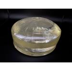
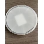
8-inch LiNbO3 wafers refer to the specific size of LiNbO3 crystal
substrates commonly used in the fabrication of optoelectronic
devices and integrated circuits. These wafers are made from
high-purity lithium niobate crystals and offer several advantages
due to their larger size. Here is a description of 8-inch LiNbO3
wafers:
- Size: 8-inch LiNbO3 wafers have a diameter of approximately 200
millimeters (8 inches), making them larger than smaller-sized
wafers like 4-inch or 6-inch wafers. The larger surface area of
8-inch wafers allows for higher device density and increased
production efficiency.
- Thickness: The standard thickness of 8-inch LiNbO3 wafers ranges
from 0.5 to 1 millimeter. However, custom thicknesses can also be
obtained based on specific application requirements.
- Crystal Orientation: 8-inch LiNbO3 wafers can be cut and oriented
along different crystal planes, typically the Y- and X-cut
orientations, which are commonly used in many optoelectronic
devices. However, other crystal orientations may also be available
depending on the specific application needs.
- Advantages: The larger size of 8-inch LiNbO3 wafers offers several
advantages:
Increased Device Capacity: The larger surface area allows for a
higher number of devices and integrated circuits to be fabricated
on a single wafer, thereby improving production capacity and yield.
Enhanced Integration: With a larger area, 8-inch wafers enable
higher device integration and improved performance due to the
availability of more real estate for components and interconnects.
Improved Uniformity: The manufacturing process for larger wafers
often results in better consistency and uniformity across the
wafer, contributing to improved device performance and yield.
- Availability: 8-inch LiNbO3 wafers are commercially available from
various specialized semiconductor material manufacturers. These
suppliers provide ready-made 8-inch wafers or offer customization
options to meet specific application requirements.
Applications:
8-inch LiNbO3 wafers find applications in various fields where
their unique optical and electro-optic properties are utilized. For
example: Optical Modulators, Frequency Conversion, Acousto-Optic
Devices, Integrated Optics, Nonlinear Optical Devices, Optical
Sensors.
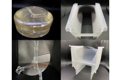
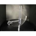
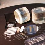
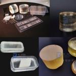
Packing and Shipping:
LiNbO3 Wafers should be packaged and shipped in accordance with the
following guidelines:
- LiNbO3 Wafers should be packaged in an antistatic bag.
- The package should be padded with cushioning material to protect
against shock.
- The package should be clearly labeled with the product name and the
contents of the package.
- The package should be sent by a reputable courier service.
- The package should be tracked and insured.