
11 - 20 of 36
idt use 8 inch wafer
Selling leads
|
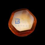
.... If the charge distribution is not symmetrical, the net polarization will appear, and an electric field will be generated, which is the piezoelect...
2024-12-09 20:34:25
|
|
... until the 1940s. The property of certain crystals to exhibit electrical charges under mechanical loading was of no practical use until very high ...
2025-06-21 11:31:50
|
|
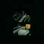
..., filters, transducers, high-frequency surface acoustic wave devices, as well as bulk acoustic devices. Material Characteristics Material 3" 4" 6" ...
2025-07-17 00:19:03
|
|
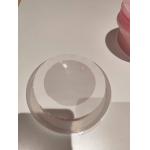
...Inch Borofloat 33 Glass Wafer For Electronics, Optics, And Semiconductors Borofloat 33 Glass Wafer Description Borofloat 33 is a type of borosilica...
2024-12-09 22:13:23
|
|
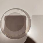
.... Such wafers are most commonly specified as 3" diameter with a reference flat. Wafer orientation is customer specified based on desired component ...
2025-07-17 00:19:03
|

|
... properties and thermal stability. It is widely used in various industries, including optics, lasers, semiconductors, and scientific research. JGS1 ...
2025-07-17 00:19:03
|
|
... or wafer made from a thin layer of LiNbO3 material. Size: The thin film has a diameter of 3 inches, which is equivalent to approximately 76 ...
2024-12-09 22:36:19
|
|
... or wafer made from a thin layer of LiTaO3 material. Size: The thin film has a diameter of 3 inches, which is equivalent to approximately 76 ...
2025-07-17 00:19:03
|
|
... lithium niobate exhibits high photorefraction. Therefore in high-power laser applications, magnesium oxide-doped crystals (MgO:LiNbO3) are used. ...
2025-07-17 00:19:03
|
|
... acoustic attenuation. Typical cut angle for SAW application is 36°Y, 42°Y, X-cut etc. The Lithium Tantalate reduction technology makes the wafer ...
2024-12-09 20:34:25
|