
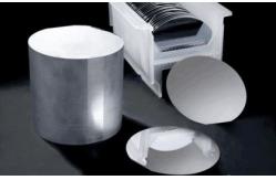
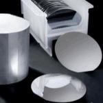
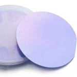
Semiconductor Silicon Wafer Prime Grade 3 Inch To 12 Inch
|
|
Semiconductor Silicon Wafer Prime Grade 3 Inch To 12 Inch
Silicon wafer is a material used for producing semiconductors, which can be found in all types of electronic devices that improve the lives of people. Silicon comes second as the most common element in the universe; it is mostly used as a semiconductor in the technology and electronic sector.
BonTek provide any diameters from 1’’ (25.4 mm) to 12’’ (300 mm) in order to provide the most flexibility as possible. With the aim of providing the largest range of specification, we work either Cz (Czochralski) or FZ (Float Zone) silicon wafers. Furthermore, in order to manufacture qualitative products, pure silicon (9N) raw material is used. The polishing process is also made internally in order to meet or exceed the Semiconductor Equipment and Materials International standards (SEMI).
Acceptance Check
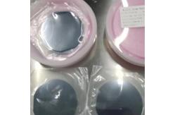
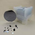
1. The product is fragile. We have adequately packed it and labeled it fragile. We deliver through excellent domestic and international express companies to ensure transportation quality.
2. After receiving the goods, please handle with care and check whether the outer carton is in good condition. Carefully open the outer carton and check whether the packing boxes are in alignment. Take a picture before you take them out.
3. Please open the vacuum package in a clean room when the products are to be applied.
4. If the products are found damaged during courier, please take a picture or record a video immediately. DO NOT take the damaged products out of the packaging box! Contact us immediately and we will solve the problem well. |
||||||||||||||||||||||||||||||||||||||||||||||||||||||||||||||||||||||||||||||||
| Product Tags: Semiconductor Silicon Wafer 12 Inch Silicon Wafer Polish Semiconductor Wafer | ||||||||||||||||||||||||||||||||||||||||||||||||||||||||||||||||||||||||||||||||
|
Phi 2'' To 8'' Thermal Oxide Silicon Wafer N-Type P-Type With An Insulating Oxide Layer |

|
Semiconductor Silicon Wafer Prime Grade 3 Inch To 12 Inch |
|
12 Inch Semiconductor Silicon Wafer Prime Test Dummy Wafers |
|
Boron Doped Phosphorus Doped Silicon Wafer With High Resistivity For Semiconductor |
|
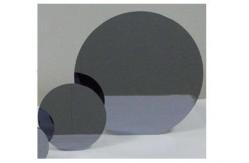
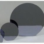
2'' To 12'' P Type N Type Silicon Wafer With High Resistivity For Semiconductor |
|
2'' To 8'' Polished Silicon Wafer In Prime, Test, Monitor, SEMI Standard |